(PR) NVIDIA's New Ampere Data Center GPU in Full Production
NVIDIA today announced that the first GPU based on the NVIDIA Ampere architecture, the NVIDIA A100, is in full production and shipping to customers worldwide. The A100 draws on design breakthroughs in the NVIDIA Ampere architecture — offering the company's largest leap in performance to date within its eight generations of GPUs — to unify AI training and inference and boost performance by up to 20x over its predecessors. A universal workload accelerator, the A100 is also built for data analytics,
NVIDIA GTC 2020 Keynote Liveblog: Ampere Takes Centerstage
NVIDIA today announced the first virtual Graphics Technology Conference, its annual tradeshow where industry partners, game developers, and HPC/AI researchers converge, and NVIDIA makes its most groundbreaking announcements. It's been close to two years since NVIDIA announced the most unexpected piece of consumer graphics technology, "Turing." This year promises to be equally big in terms of technology reveal, with "Ampere." The event is expected to commence with a keynote address by CEO Jensen Huang. 

NVIDIA "Ampere" Designed for both HPC and GeForce/Quadro
NVIDIA CEO Jensen Huang in a pre-GTC press briefing stressed that the upcoming "Ampere" graphics architecture will spread across both the company's compute-accelerator and commercial graphics product lines. The architecture makes its debut later today with the Tesla A100 HPC processor for breakthrough AI acceleration. It's unlikely that any GeForce products will be formally announced this month, with rumors pointing to a GeForce "Ampere" product launch at a gaming-focused event in September, close to "Cyberpunk 207
NVIDIA Tesla A100 "Ampere" AIC (add-in card) Form-Factor Board Pictured
Here's the first picture of a Tesla A100 "Ampere" AIC (add-in card) form-factor board, hot on the heals of the morning big A100 reveal . The AIC card is a bare PCB, which workstation builders will add compatible cooling solutions on. The PCB features the gigantic GA100 processor with its six HBM2E stacks, in the center, surrounded by VRM components, and I/O on three sides. On the bottom side,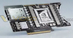
MSI B550 Motherboard Lineup Hits the Radar
MSI registered five new motherboard SKUs with the Eurasian Economic Commission, based on the AMD B550 chipset. The five new socket AM4 motherboards cover a wide range of sub-$200 (expected) price-points. The lineup is led by the MSI Performance Gaming (MPG) B550 Gaming Carbon WiFi, which was part of AMD's chipset reveal presentation ; followed closely by the MPG B550 Gaming Edge WiFi, its Mini-ITX sibling, the MPG B
ASUS Expects a Massive 30% Surge in Notebook Shipments in Q2-2020
With the COVID-19 global pandemic forcing entire payrolls to work from home, the demand for pre-built computers handed out by companies, or those purchased by workers at their own expense, has hit an all time high. ASUS expects a massive 30% surge in notebook shipments in Q2-2020, with Q1 having mopped up inventories across the globe. For Q1-2020, ASUS reported $2.12 billion in revenues, down 28.
(PR) ASUS Announces the W480 Workstation Series
ASUS today announced the W480 series workstation motherboard and workstation system designed to showcase the full potential of the latest Intel Xeon W-1200 processors. The ASUS W480 workstation series is the ideal choice for small-to-medium businesses and content creators seeking workstations delivering essential performance along with professional-grade reliability and security at a budget friendly price.
Teamed up with the latest Intel Xeon W-1200 processors featuring up to 10 cores, 20 threads, 5
Teamed up with the latest Intel Xeon W-1200 processors featuring up to 10 cores, 20 threads, 5
NVIDIA Ampere A100 Has 54 Billion Transistors, World's Largest 7nm Chip
Not long ago, Intel's Raja Koduri claimed that the Xe HP "Ponte Vecchio" silicon was the "big daddy" of Xe GPUs, and the "largest chip co-developed in India," larger than the 35 billion-transistor Xilinix VU19P FPGA co-developed in the country. It turns out that NVIDIA is in the mood for setting records. The "Ampere" A100 silicon has 54 billion transistors crammed into a single 7 nm die (not counting transistor
NVIDIA Tesla A100 GPU Pictured
Thanks to the sources of VideoCardz, we now have the first picture of the next-generation NVIDIA Tesla A100 graphics card. Designed for computing oriented applications, the Tesla A100 is socketed GPU designed for NVDIA's proprietary SXM socket. In a post few days ago, we were estimating that you might fit Tesla A100 GPU in the socket of the previous Volta V100 GPUs as it is a similar SXM socket. However, the mounting holes have been re-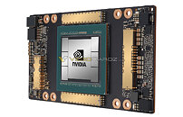
(PR) Google Chrome Beta Receives Tab Grouping Feature
There are two types of people in the world: tab minimalists who have just a few tabs open at a time and tab collectors who have...significantly more. For minimalists and collectors alike, we're bringing a new way to organize your tabs to Chrome: tab groups. This feature is available now in Chrome Beta. Now, with a simple right click, you can group your tabs together and label them with a custom name and color. Once the tabs are grouped together, you can move and