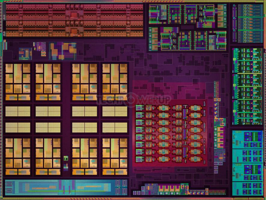
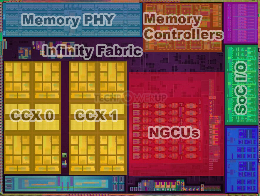
"Renoir" features 8 CPU cores based on the "Zen 2" microarchitecture, divided into two 4-core CCXs (CPU complexes). Unlike on 8-core chiplets meant for "Matisse" or "Rome" MCMs, the "Renoir" CCX only features 4 MB of shared L3 cache, probably because latencies to the memory controller are low enough. The L2 cache per core is unchanged at 512 KB. The "total cache" (L2 + L3 on silicon) adds up to 12 MB. The iGPU of "Renoir" is a hybrid between "Vega" and "Navi." The SIMD components are carried over from "Vega," while the display- and multimedia engines are from "Navi." The iGPU features 8 NGCUs that add up to 512 stream processors. Infinity Fabric covers much of the die area, connecting the various components on the die. AMD introduced a new dual-channel integrated memory controller that supports LPDDR4x at up to 4233 MHz, and standard DDR4 up to 3200 MHz.