Intel has overcome one big challenge that will lead to the creation of hyper-large chips beyond 12x reticle size through advanced packaging technologies.
Modern-day chips don't rely on a single piece of silicon, and instead utilize a range of silicon dies, interconnected together using the latest packaging solutions. The terminology used for such designs is chiplets, and chiplets were made to overcome scaling bottlenecks and the growing demand for compute.
Inside Intel's Rio Rancho, New Mexico facilities, advanced packaging technologies are expanding the "reticle limit"—scaling packages to 8x the industry standard today, and over 12x by 2028.
We’ve moved past the era of one big chip to a system of chips, almost like a “silicon mosaic”, where specialized tiles are interconnected in a single, massive package.
“Back in the 1980s this site was the leader in 6-inch wafer manufacturing. Now over 40 years later, things have flipped and this site is the leader in the United States for advanced packaging,” explains Katie Prouty, manager of Intel’s Fab 9 advanced packaging facility in New Mexico.
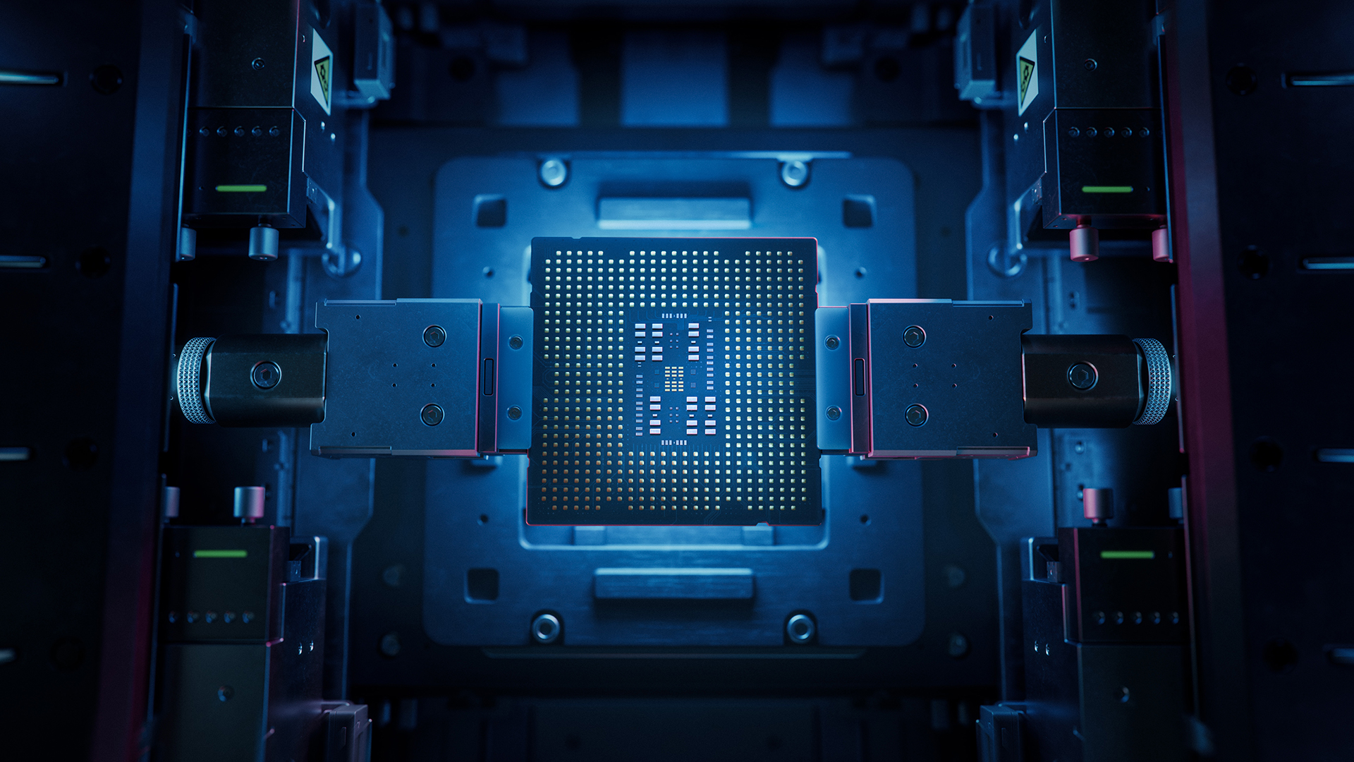
But today's packaging technologies also have their own limitations on the number of chiplets that can be accommodated on a single package. To overcome these, semiconductor companies are working on several new solutions, and Intel is pioneering in this segment with its own advanced packaging solutions with technologies such as EMIB and Foveros . These technologies enable the creation of chips that offer more compute performance through larger, flexible, scalable, & cost-effective designs.
Now, Intel is going one step ahead towards the development of what it is calling hyper-large form factor (HLFF) packages. These ultra-large chip packages will measure 240mm x 240mm, achieving a 24x reticle size that is bigger than anything that the industry has seen yet besides panel-level packages.
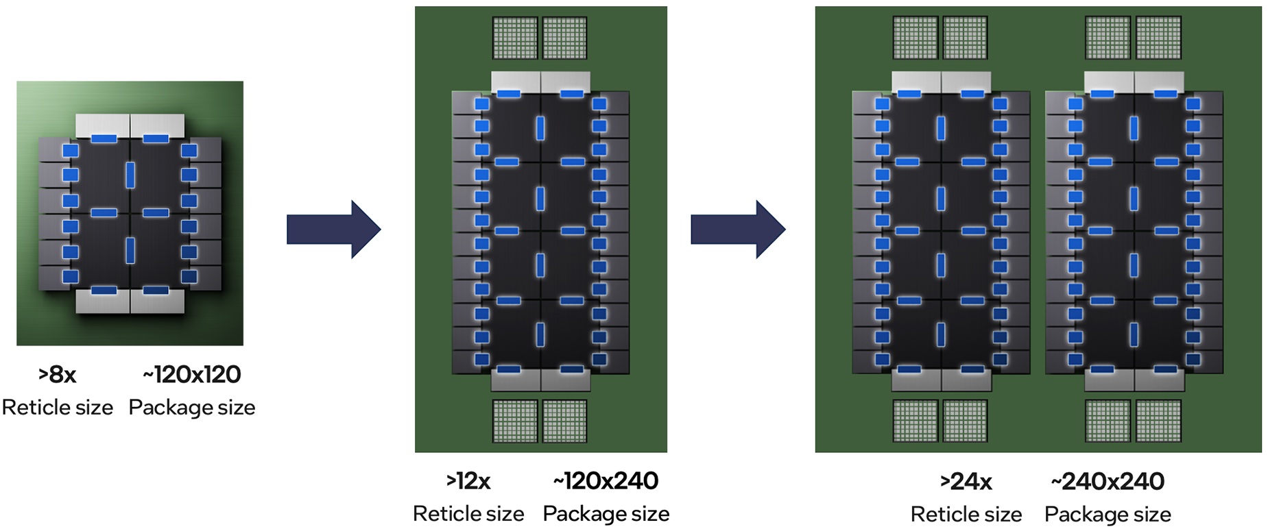
To achieve this, Intel's research team and engineering team developed material & process innovations to enable reliable encapsulation at these larger scales. Some of the key challenges of achieving such large packages include:
- Moving data fast enough. Inside the package, EMIB-T bridges with metal layers finer than 2 micrometers (µm) enable the 64 Gb/s per channel speeds AI workloads require for chip-to-chip and chip-to-memory connections. For communication leaving the package, the research evaluates co-packaged copper cable connectors and co-packaged optics as the leading approaches for reaching the industry's projected next off-package speed target of 448 Gb/s.
- Delivering power efficiently. Routing power from the package edges becomes increasingly inefficient at HLFF scale. The research proposes embedding silicon capacitors within the substrate and directly beneath the chips, providing up to 1 millifarad (mF) of local energy storage per full reticle chip area. Moving voltage regulators onto or into the package also lets them respond faster to changing chip power demands.
- Building redundancy for yield. The team proposes adding spare communication lanes alongside active ones. Adding just three to four spare lanes to every group of 64 raises bundle yield from about 97% to above 99%. At HLFF scale, this difference is key to making products economically manufacturable.
- Keeping the package flat. The research team modeled free-standing warpage of up to 7 mm at room temperature, enough to disrupt electrical connections and thermal contact. The proposed solution combines thick stiffener rings, low-expansion glass-core substrates, and a multi-ball solder ball process. During operation, pressing the cooling hardware down with force above approximately 4,500 newtons (N) helps keep the package nearly flat.
- Managing heat at kilowatt scale. HLFF packages are expected to operate at 15 to 25 kilowatts (kW) total, with localized hot spots that demand aggressive cooling. Instead of one large cold plate, the research proposes a modular, cell-based cooling architecture with independently controlled thermal zones and embedded sensors, designed to scale beyond 5 kW of cooling per module.
A bigger challenge was encapsulation, which is the process of sealing the chip with a protective layer, but as chip and package sizes grow, this becomes harder. The underfill material that flows and seals the joints between the chips and the substrate. The reason why this process is harder at larger scales is that the sealant has to travel a larger distance.
Currently, the maximum distance the underfill can flow is around 43mm with EMIB, and 22mm with standard package designs. But when you talk about 5x-10x reticle scales, the underfill has to reach much larger distances. The distances also add more resistance, making it harder to remove air pockets and voids.
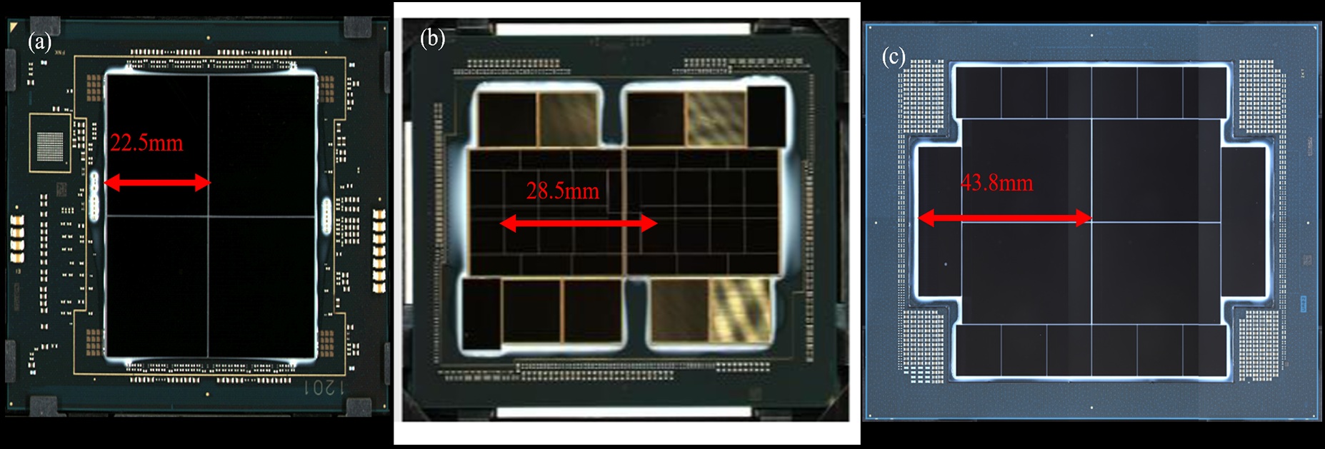
Intel Foundry has come up with a solution to solve this encapsulation problem through "three coordinated levers: material, dispense strategy, and cure."
The first step is to use an optimized underfill material that balances flow and reliability. Viscosity is lowered so that the material can flow a longer distance. Intel developed a direct flow test on representative package vehicles to identify formulations that extend flow without sacrificing mechanical integrity.
The second step was to redesign the dispensing strategy by relying on a multi-point application rather than edge-dispensing. This improves coverage and reduces the effective flow distance.
And lastly, the cure process has been tuned to eliminate defects that occur after dispensing. Intel uses optimized cure conditions to collapse voids, which in turn lead to packages with "void-free" designs.
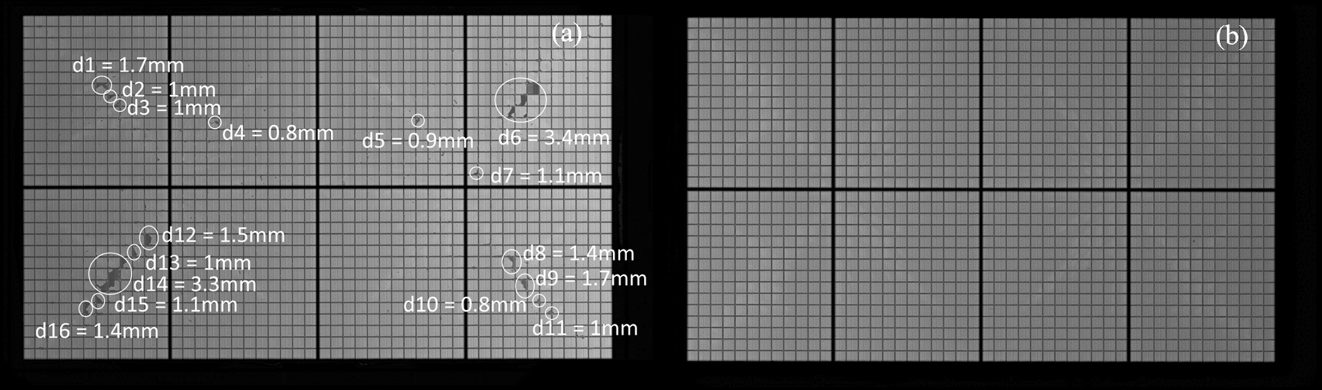
With all of this, Intel was able to validate several packages aligned with its HLFF (Hyper-Large Form Factor) chip architectures. These include an EMIB-based package exceeding 5x reticle. The chip housed 18 dies, which include 12 HBM sites, and achieved void-free encapsulation at flow distances of up to 40mm.
Intel also validated a larger tiled EMIB package beyond 7x reticle with void-free results. Using the Foveros 3D packaging solution, void-free encapsulation was successfully achieved at 2x and 4x reticle scales, and 2x passed "full reliability testing".
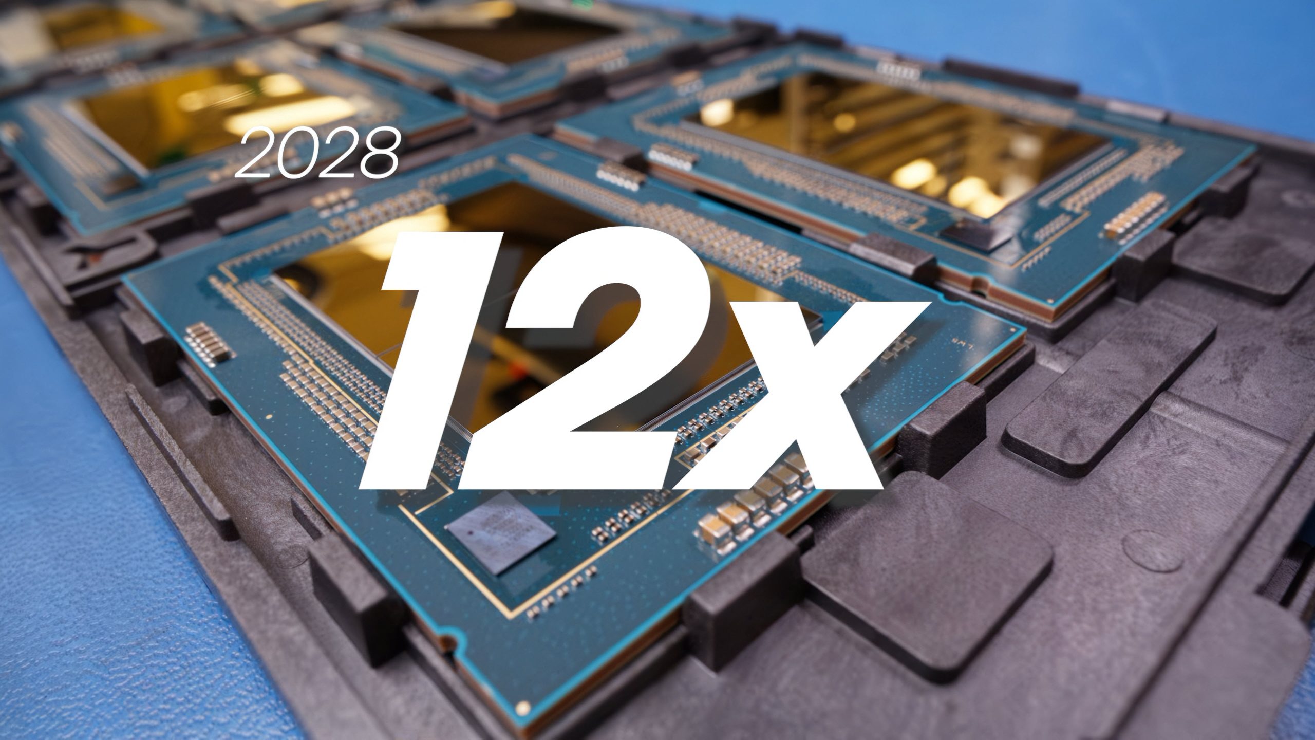
As Intel continues to accelerate its advanced packaging solutions, the company will continue to push encapsulation past 7x reticle sizes, with the roadmap scaling beyond 12x reticle in the near term and panel-level packages taking things past 50x reticle.
Intel and TSMC are going all-out in the panel-level packaging segment , with Rio Rancho's glass substrates being a key enabler of hyper-large chips, which will deliver an unprecedented increase in compute performance, while offering world-class efficiency at scale.
Follow Wccftech on Google to get more of our news coverage in your feeds.