Samsung has introduced brand new memory and storage technologies at FMS 2026, such as V10 BV-NAND, zHBM, and zNAND-O .
As AI and compute requirements continue to grow, the current swath of technologies is starting to see drawbacks, requiring manufacturers to invest in transformative concepts that are going to play a fundamental role in future AI infrastructure.
At FMS 2026, Samsung displayed two brand new technologies that are currently in concept stage, but would become a major deal moving forward if brought to life and implemented on real silicon, such as AI accelerators.
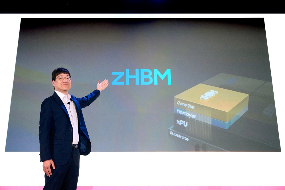
The main technology highlighted is the zHBM memory solution. According to the company, zHBM takes the existing HBM design and places it directly above the AI accelerator. Currently, HBM is featured next to the main AI accelerator compute die, but having it on top of the AI accelerator is going to save space and offer better gains when it comes to data transfer speeds.
zHBM is expected to deliver higher bandwidth and improved power efficiency. The company claims that zHBM will deliver an 8x performance leap over a conventional HBM5 solution , and over 10x gain in memory density while offering 3x the energy efficiency & cutting down thermal resistance by more than half.
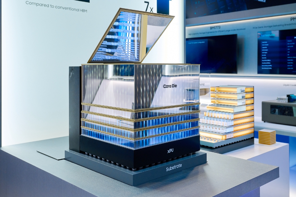
Samsung has reasons for not going into specifics of the tech since it's still in an early concept phase, but they do state that zHBM will offer flexibility in terms of customer-specific designs. Samsung is already working with its customers to further optimize the integration of zHBM on next-generation AI accelerators.
The second technology that is being unveiled is called zNAND-O, which is a high-performance and next-gen NAND solution built on the foundation of Samsung's V-NAND.
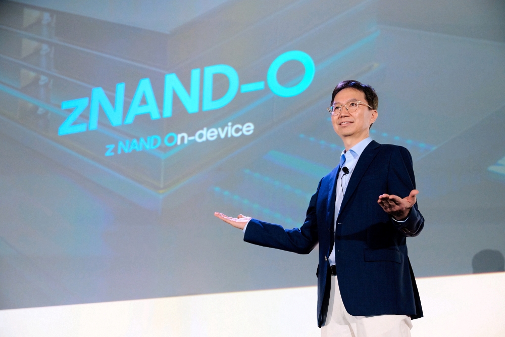
This will come in 4- and 8-layer configurations and will combine high space efficiency, improved I/O performance, and low latency. zNAND O is designed for edge AI applications, though it isn't stated if this is the multi-stacked V-NAND tech that will be ready around 2030.
And lastly, we have Samsung's next-generation NAND solution called V10 BV-NAND. This is going to be Samsung's first V-NAND architecture with hybrid bonding & takes NAND beyond 400 layers.
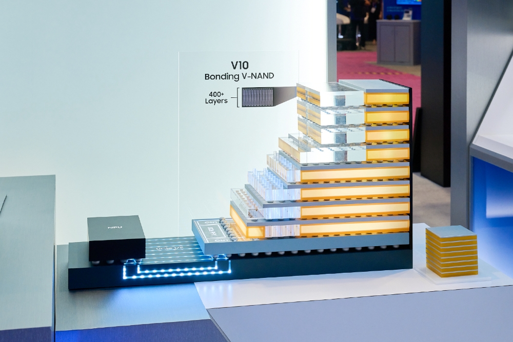
It is said that with BV-NAND, Samsung's V10 storage designs will offer higher performance and power efficiency while boosting storage density massively. The technology is straightforward, leveraging hybrid bonding to stack memory cells together instead of making a single cell with denser layers. Memory density sees a 58% boost versus V9 NAND, and also improves read, write, and IO performance versus prior generations.
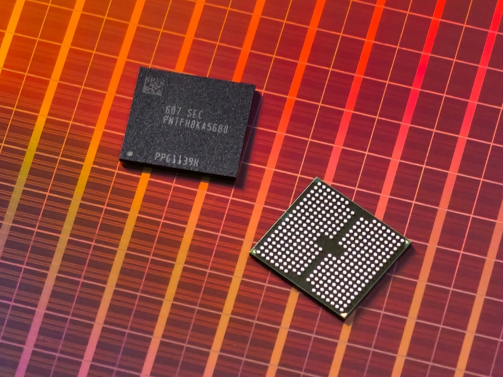
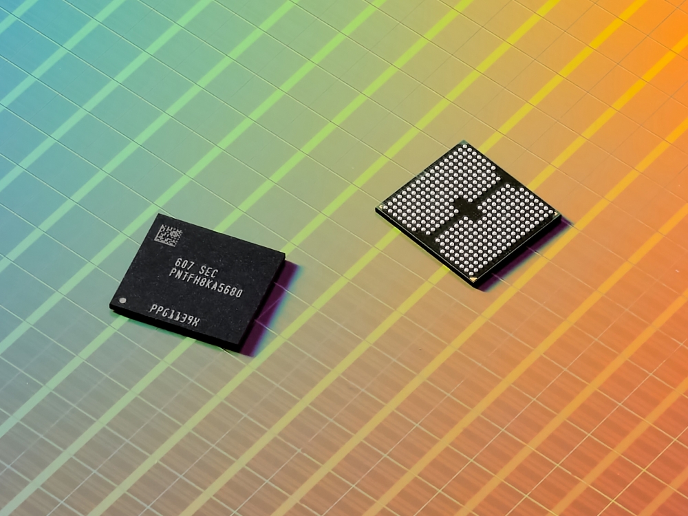
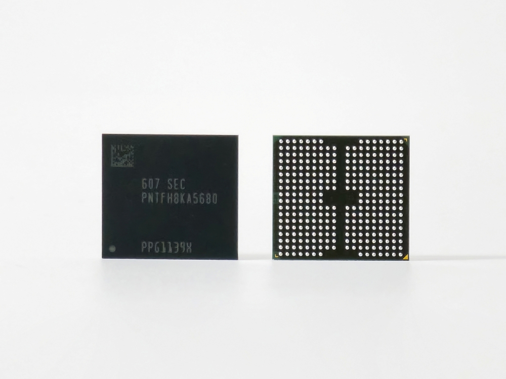
We should mention that Samsung is already planning for 1000+ layers with hybrid bonding approaches, and BV-NAND has officially kicked off this trend. In the coming years, we are going to see a rapid increase in storage capacity across Samsung's SSD and Storage portfolio, while its memory solutions see a rapid and innovative pace with technologies such as zHBM, HBM4E, HBM5, GDDR7, and beyond.
Follow Wccftech on Google to get more of our news coverage in your feeds.