Korean chip manufacturer Samsung is planning to introduce high-NA extreme ultraviolet (EUV) lithography into its production facilities to manufacture chips with the 1-nanometer manufacturing process node. The report comes courtesy Samsung Electronics' VP of Technology, ChangMin Park, and it adds that Samsung will rely on the latest lithography machines for volume production of the chips. These chips could enter mass production as early as 2030, with the Samsung executive outlining the details at a conference held in Korea.
Advances in semiconductor fabrication create limits when circuit sizes become smaller. Smaller circuit sizes depend on the wavelength of light being used, and as chip manufacturers face off with reduced sizes, they hit a fundamental limit that cannot be overcome unless the wavelength is reduced. However, the numerical aperture of the lens system used in the machinery aids manufacturers, as a higher aperture allows them to reduce the size of the circuits being printed.
On this front, while typical EUV machines are limited by the wavelength of light at 13.5 nanometers, higher aperture lenses allow manufacturers to print smaller circuits. This comes into play when planning for manufacturing next-generation chip fabrication technologies, such as 1-nanometer nodes that are typically referred to in Angstrom terms, with one angstrom equivalent to 0.1 nanometers.
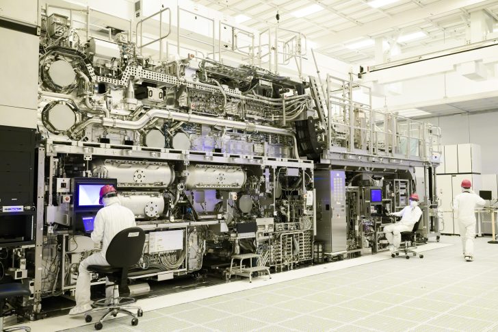
Now, while ASML's High NA EUV machines, with a numerical aperture of 0.55NA, started shipping a couple of years back, their implementation appears to be delayed once again. The first such signal came from TSMC, with reports from last year suggesting that the Taiwanese firm was considering alternatives such as photomask pellicles s, to make more advanced chips instead of using high-NA EUV machines.
Similarly, Samsung Electronics' VP of Technology, ChangMin Park, outlined in Korea earlier today that his firm will use the High NA EUV machines for technologies starting at the 1-nanometer manufacturing node. Park made the remarks at the 2026 Next-Generation Lithography + Patterning Conference and outlined that the firm had expected to use the machines for volume production of the 2-nanometer and 1.4-nanometer process nodes.
He added that Samsung believes that the machines will become necessary for nodes starting from A10 (1-nanometer) and future nodes. High NA EUV machines, through enabling smaller circuit sizes, enable printing through a single pattern. Without the higher aperture, traditional, low NA EUV machines require multi-patterning, which increases the costs, complexity and defects in the end product.
Follow Wccftech on Google to get more of our news coverage in your feeds.