The Taiwan Semiconductor Manufacturing Company (TSMC) has achieved 98% yield for some of its CoWoS packaging products, according to the firm's Vice President of Advanced Packaging Technology and Services, Ho Chun. As reported by the Economic Daily, Ho outlined that the high yield is for several AI-related products packaged through CoWoS and it involves the technology that relies on a 5.5x reticle size.
When it comes to manufacturing AI chips, lithography is just one part of the process, even though it might be among the most complex steps . The end-stage product used in data centers relies on several compute chips stitched together with memory chips as part of a final chip package. This package is typically larger than the singular chip, and firms such as TSMC use numerical terms describing the package's size.
TSMC's latest CoWoS packaging technology is able to create a final package that is 5.5 times as large as a single chip manufactured through the lithography process. Since this process requires multiple chips to be joined together, the larger area of the package compared to the chips also means that the probability of defects in the end product is higher. Some common defects include air bubbles in the underfill and bump misalignment.
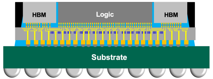
Now, TSMC's Vice President of Advanced Packaging Technology and Services, Ho Chun, has confirmed that his firm has achieved as much as a 98% to 99% yield with several AI products assembled through the CoWoS 5.5x process. According to the Economic Daily, TSMC plans to continue to expand its packaging capabilities and plans to expand its technology to 14x by 2029.
The executive also discussed the problems that companies encounter when expanding packaging capabilities to more than three times the photomask size. The photomask size determines the unit size of a single chip and, as explained above, packaging involves stitching these chips together.
According to Ho, heat tolerance and other parameters of the chips inside a package have to meet and exceed automotive standards as the package size moves beyond 3x. He added that the components inside a chip package must be prepared to meet the mechanical, thermal and other requirements of the package during the development stage in order to ensure smooth performance post-packaging.
Follow Wccftech on Google to get more of our news coverage in your feeds.