Update - Google's Vice President of Hardware, Peng Yu-Chun, has confirmed to Economic Daily News that all Pixel 11 models ship with the 3nm Tensor G6. Given that the Tensor G5 utilized the 3nm N3P technology, Google likely stuck with this lithography.
It would be considered an achievement of the ages if the Tensor G6 were announced as Google’s and the smartphone industry’s first 2nm SoC. However, even after the Pixel 11 lineup’s unveiling is over and pre-orders have kicked off, we have zero confirmation on the SoC’s lithography, so we dug around and, based on what we could gather, we could have some disappointing news.
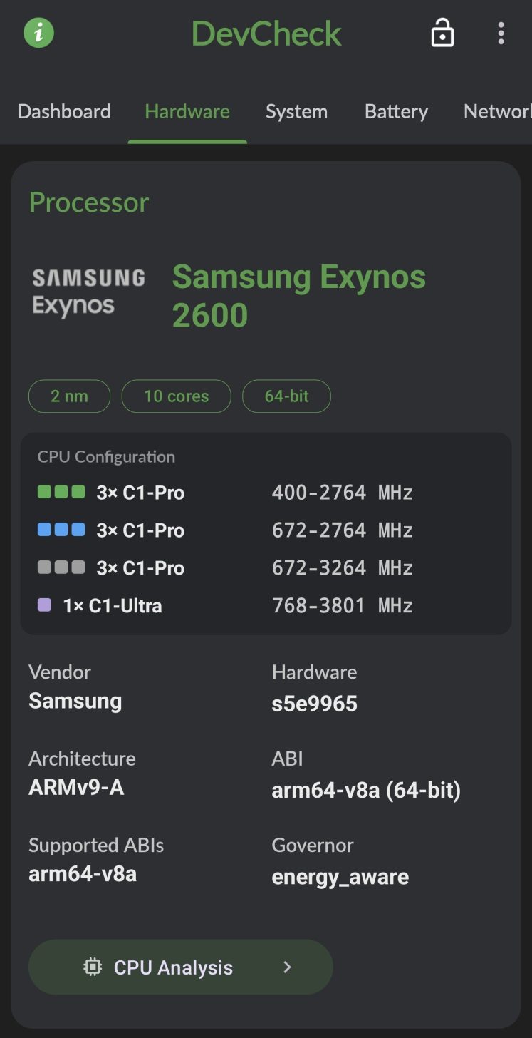
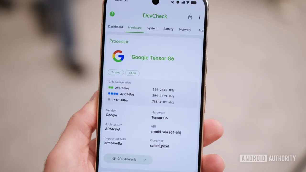
For those who don’t know, DevCheck is an Android app that provides all relevant information about your smartphone, including which manufacturing process was used for the SoC. For instance, @borntoFLY11135 shares a screenshot of the Exynos 2600 , and it is clearly mentioned as a 2nm SoC. However, the image from Android Authority only lists the 7-core CPU cluster, but nothing regarding its lithography.
Typically, a software update from DevCheck will remedy this problem, but even if these details aren’t mentioned in the app, Google hasn’t made any claims about the 2nm node either. Launching a chipset on advanced lithography should be a joyous moment for any company, but seeing Google omit this information is suspicious.
The company has mentioned that the Tensor G6 CPU delivers up to 20 percent better power efficiency, and while this claim could mean a better manufacturing process, you need to be reminded that Google removed one CPU core from the configuration, which would lead to better battery life at the expense of multi-core performance.
Meanwhile, an upgraded CPU delivers up to 20% better power efficiency to take you through your day. And together with the new Titan M3 security chip, Google Tensor G6 helps protect your data.
To be fair, it is understandable if Google sticks with TSMC’s 3nm N3P process since, not only does the company ship a small number of Pixel smartphones each year, but choosing TSMC’s 2nm lithography would make little sense from a financial perspective. The Mountain View behemoth doesn’t target peak performance or record efficiency with its Tensor G6, so adopting the 2nm node would be a wasteful decision.
Google did, however, pack a 50 percent more capable TPU for better on-device AI performance, but you don’t necessarily need to take advantage of TSMC’s cutting-edge lithography. We’d honestly be surprised if DevCheck later reveals that the Tensor G6 is made on the 2nm process.
Follow Wccftech on Google to get more of our news coverage in your feeds.