Korean chip giant Samsung might repurpose a production line at an under-construction research and development facility to manufacture base logic dies for its HBM memory chip production. The report comes courtesy of industry sources quoted by ZDNet, and it adds that since the facility's opening is roughly scheduled in two years, the plans are subject to revision.
The design of HBM memory chips, which are used primarily in AI computing applications, requires multiple DRAM memory chips stacked on top of each other. As the performance requirements of computing infrastructure grow, the design of these chips is also evolving. Along with the number of DRAM layers stacked on top of each other, another key factor that is evolving is the base die on the HBM memory chips.
The first update to the bae die occurred when manufacturers advanced to HBM3 and HBM3E memory chips. This upgrade saw manufacturers jump to IC foundry node processes for the base die for the first time as data rates and pin speeds increased significantly from the previous generation of memory chips. As a result, the base die started to rely on logic nodes ranging from 20-nanometers to 12-nanometers.
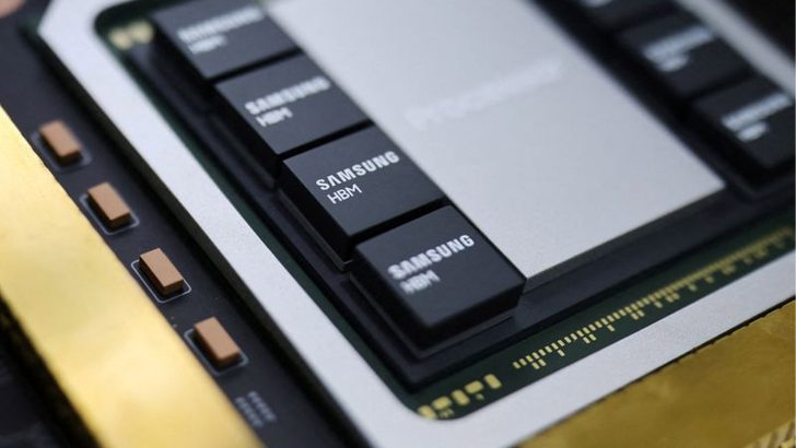
The next shift occurred with the HBM4 memory chips that are currently used in the latest AI products, such as NVIDIA's Rubin chips. It was necessitated by high data rates achieved by HBM3E memory and wider buses and more through-silicon vias (TSVs). These shifts saw foundries, such as TSMC and Samsung Foundry, take over the role of manufacturing the HBM chip base die.
Now, a report from ZDNet claims that Samsung is interested in repurposing a production line at its under-construction research and development facilities in Korea's Giheung industrial district. This line can be used to manufacture HBM base dies through the 2-nanometer chip manufacturing technology, says the report. It adds that the base dies might be destined for NVIDIA's AI chips and the line that might be used for this purpose is the NRD-K Line 2.
Earlier this year, Samsung announced that it would use the 4-nanometer manufacturing technology for the HBM4 memory chips. Along with Samsung, SK hynix will also work with a foundry for its HBM chips, as the firm has teamed up with TSMC. TSMC offers both the mature N12 node and the advanced N5 node as options for building HBM memory chips. The third player in the memory industry, Micron, has also partnered up with TSMC for its HBM4 memory chips.
Follow Wccftech on Google to get more of our news coverage in your feeds.