AMD Instinct MI200 pictured
AMD’s first multi-chip-module general-purpose graphics processor (GPGPU) has been leaked ahead of launch.
ExecutableFix has leaked the photo of the actual Instinct MI200 compute accelerator.
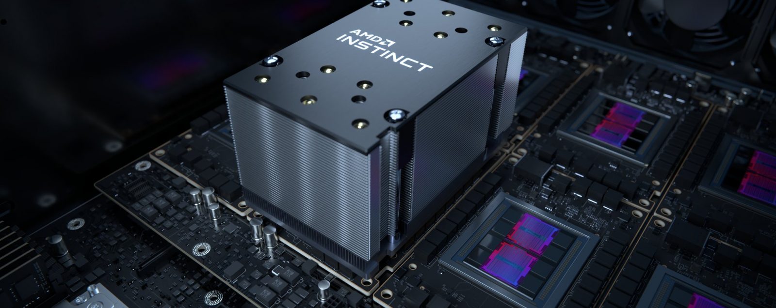
AMD Instinct MI200, Source: ExecutableFix
The render appears to confirm it is a dual die design with as many as 8 HBM stacks. According to rumors, the GPU is to feature up to 110 Compute Units and 128 GB of HBM2e memory.
What might be interesting to note is that the packaging of dual-die Aldebaran GPU is nearly identical to TSMC CoWoS-3 (Chip on Wafer on Substrate):
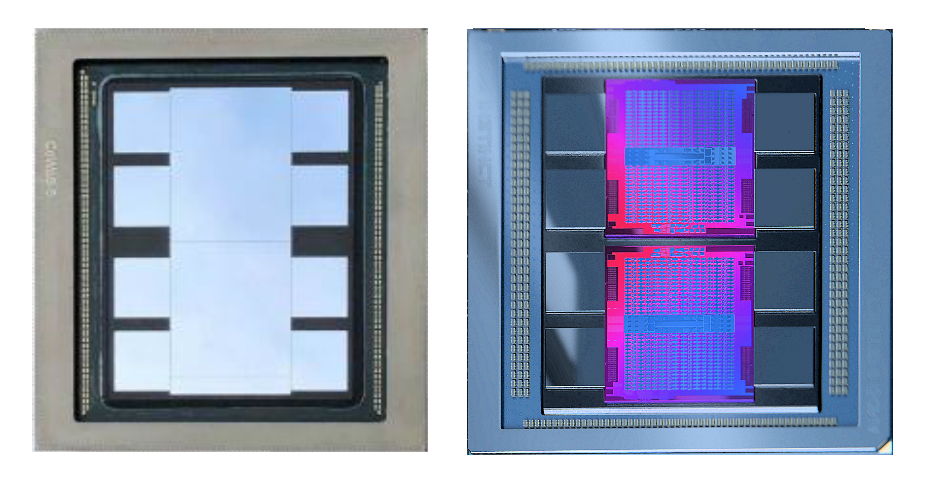
TSMC CoWoS-3 vs AMD Aldebaran GPU, Source: VideoCardz/ExecutableFix
AMD is announcing its MI200 GPGPU just a day ahead of NVIDIA GTC 2021 Keynote, where its CEO is expected to unveil the first details on its next HPC architecture known as Hopper.
| RUMORED AMD Instinct Accelerators Specifications | ||||
|---|---|---|---|---|
| VideoCardz | AMD Radeon Instinct MI60 | AMD Instinct MI100 | AMD Instinct MI250 | AMD Instinct MI250X |
| Architecture | 7nm GCN5 (GFX906) | 7nm CDNA1 (GFX908) | 6nm CDNA2 (GFX90A) | 6nm CDNA2 (GFX90A) |
| GPU | Vega 20 | Arcturus | Aldebaran (MCM) | Aldebaran (MCM) |
| Compute Tiles | 1 | 1 | 2 | 2 |
| Compute Units | 64 | 120 | 208 | 220 |
| GPU Clock Speed | 1800 MHz | ~1500 MHz | ~1700 MHz | ~1700 MHz |
| FP16 Compute | 29.5 TFLOPS | 185 TFLOPS | 362 TFLOPS | 383 TFLOPS |
| FP32 Compute | 14.7 TFLOPS | 23.1 TFLOPS | 45.3 TFLOPS | 47.9 TFLOPS |
| FP64 Compute | 7.4 TFLOPS | 11.5 TFLOPS | 47.9 TFLOPS | 47.9 TFLOPS |
| VRAM | 32 GB HBM2 | 32 GB HBM2 | 128 GB HBM2E | 128 GB HBM2E |
| Memory Clock | 2.0 Gbps | 2.4 Gbps | 3.2 Gbps | 3.2 Gbps |
| Memory Bus | 4096-bit | 4096-bit | 8192-bit | 8192-bit |
| Memory Bandwidth | 1 TB/s | 1.23 TB/s | 3.2 TB/s | 3.2 TB/s |
| Form Factor | Dual Slot, Full Length | Dual Slot, Full Length | OAM | OAM |
| Cooling | Passive Cooling | Passive Cooling | Passive Cooling | Passive Cooling |
| TDP | 300W | 300W | 560W | 560W |