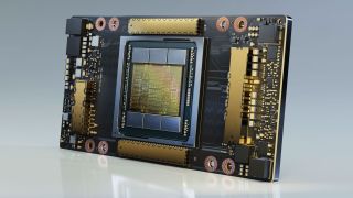
The day has finally arrived for Nvidia to take the wraps off of its Ampere architecture . Sort of. While Ampere will inevitably make its way into some of the best graphics cards and find a place on our GPU hierarchy , today's digital GTC announcement is only about the Nvidia A100, a GPU designed primarily for the upcoming wave of exascale supercomputers and AI research. It's the descendant of Nvidia's existing line of Tesla V100 GPUs, and like Volta V100 we don't expect to see A100 silicon in any consumer GPUs. Well, maybe a Titan card—Titan RTX 3000?—but I don't even want to think about what such a card would cost, because the A100 is a behemoth of a chip.

Let's start with what we know at a high level. First, the Nvidia A100 will pack a whopping 54 billion transistors, with a die size of 826mm square. GV100 for reference had 21.1 billion transistors in an 815mm square package, so the A100 is over 2.5 times as many transistors, while only being 1.3% larger. Nvidia basically couldn't make a larger GPU, as the maximum reticle size for current lithography is around 850mm square. The increase in transistor count comes courtesy of TSMC's 7nm FinFET process, which AMD, Apple, and others have been using for a while now. It's a welcome and necessary upgrade to the aging 12nm process behind Volta.
Along with the monster GPU itself are six stacks of HBM2 memory, which Nvidia says provide 40GB of total memory capacity. Since HBM2 stacks come in power of two size increments (i.e., 8GB per stack), we can only assume one of the stacks is for either ECC or redundancy of some form. For HPC (high performance computing) nodes in a super computer, Nvidia also upgraded the NVLink to 600GB/s for each GPU, and NVSwitch provides full speed connections to any other node in a server. 8-way Nvidia A100 systems already exist and have been shipped to customers including the Department of Energy.
The Nvidia A100 isn't just a huge GPU, it's the fastest GPU Nvidia has ever created, and then some. The third generation Tensor cores in A100 provide a new hybrid FP32 format called TF32 (Tensor Float 32) that aims to provide a balanced option with the precision of FP16 and exponent sizes of FP32. For workloads that use TF32, the A100 can provide 312 TFLOPS of compute power in a single chip. That's up to 20X faster than the V100's 15.7 TFLOPS of FP32 performance, but that's not an entirely fair comparison since TF32 isn't quite the same as FP32.
Elsewhere, the A100 delivers peak FP64 performance of 19.5 TFLOPS. That's more FP64 performance than the V100's FP32, and about 2.5 times the FP64 performance. Interestingly, Nvidia says elsewhere that the third generation Tensor cores support FP64, which is where the 2.5X increase in performance comes from, but details are a scarce. Assuming the FP64 figure allows similar scaling as previous Nvidia GPUs, the A100 will have twice the FP32 throughput and four times the FP16 performance—39 TFLOPS and 78 TFLOPS, respectively. But Nvidia hasn't revealed any details on the Tensor core or CUDA core configuration yet.
Let's reiterate that this GPU is not going into GeForce any time soon. Asked about the consumer line, Nvidia CEO Jensen Huang noted that Nvidia doesn't use HBM2 in consumer parts. We can safely assume there will be GDDR6-equipped Ampere GPUs at some point, but they won't be using the A100 silicon. Which, again, is fair enough. 826mm square and 40GB HBM2 (with presumably around 1.35 GBps of bandwidth) isn't something our consumer PCs really need right now, never mind the FP64 and TF32 clusters.
One interesting tidbit that never came up in the announcement: ray tracing. The Volta V100 also skipped ray tracing, partly because it came before Turing but also because it was focused on delivering compute above all else. It seems likely the A100 will follow a similar path and leave RT cores for other Ampere GPUs. That's conjecture, and it could be Nvidia just wasn't focusing on ray tracing for this initial announcement, but if correct it's yet another clear indication that A100 isn't for consumers and probably won't even go into a Titan card. Or maybe we'll get a Titan A100 for entry-level compute and deep learning or whatever.
The Nvidia A100 should definitely deliver the goods for the target market, though. Along with other architectural enhancements including sparse matrix optimizations where it's twice as fast as V100, the A100 can be has multi-GPU instancing that allows it to be partitioned into seven separate instances. For scale-out applications, then, a single A100 can have 7X the instancing performance of a V100 GPU.
Of course, supercomputers wouldn't just want a single A100 card, and while those will exist (for inference and instancing applications, among others), the real power comes in the form of the new Nvidia DGX A100. Packing eight A100 GPUs linked via six NVSwitch with 4.8 TBps of bi-directional bandwidth, it can in effect behave as a single massive GPU with the right workloads. The eight GPUs can also provide 10 POPS (PetaOPS) of INT8 performance, 5 PFLOPS of FP16, 2.5 TFLOPS of TF32, and 156 TFLOPS of FP64 in a single node. And all this can be yours, for only $199,000—well, it could be at some point, as the waiting list is probably already quite long.
Need even more performance? Say hello to the Nvidia DGX A100 Superpod. Housing 140 DGX A100 systems, each with eight A100 GPUs (1,120 total A100 GPUs), the A100 Superpod was built in under three weeks and delivers 700 PFLOPS of AI performance. Nvidia has added four such superpods to its Saturn V supercomputer, which previously had 1,800 DGX-1 systems with 1.8 ExaFLOPS of compute. Adding just 560 DGX A100 systems tacks on another 2.8 ExaFLOPS, for a total of 4.6 ExaFLOPS.
All of this is great news for supercomputer and HPC use, but it leaves us with very little information about Nvidia's next generation Ampere GPUs for consumer cards. We know that Nvidia crammed in 2.5 times as many transistors in roughly the same die space, which means it could certainly do the same for consumer GPUs. Remove some of the FP64 and deep learning functionality and focus on ray tracing and graphics cores, and the resulting GPU should be very potent. We'll find out just how potent in the coming days.