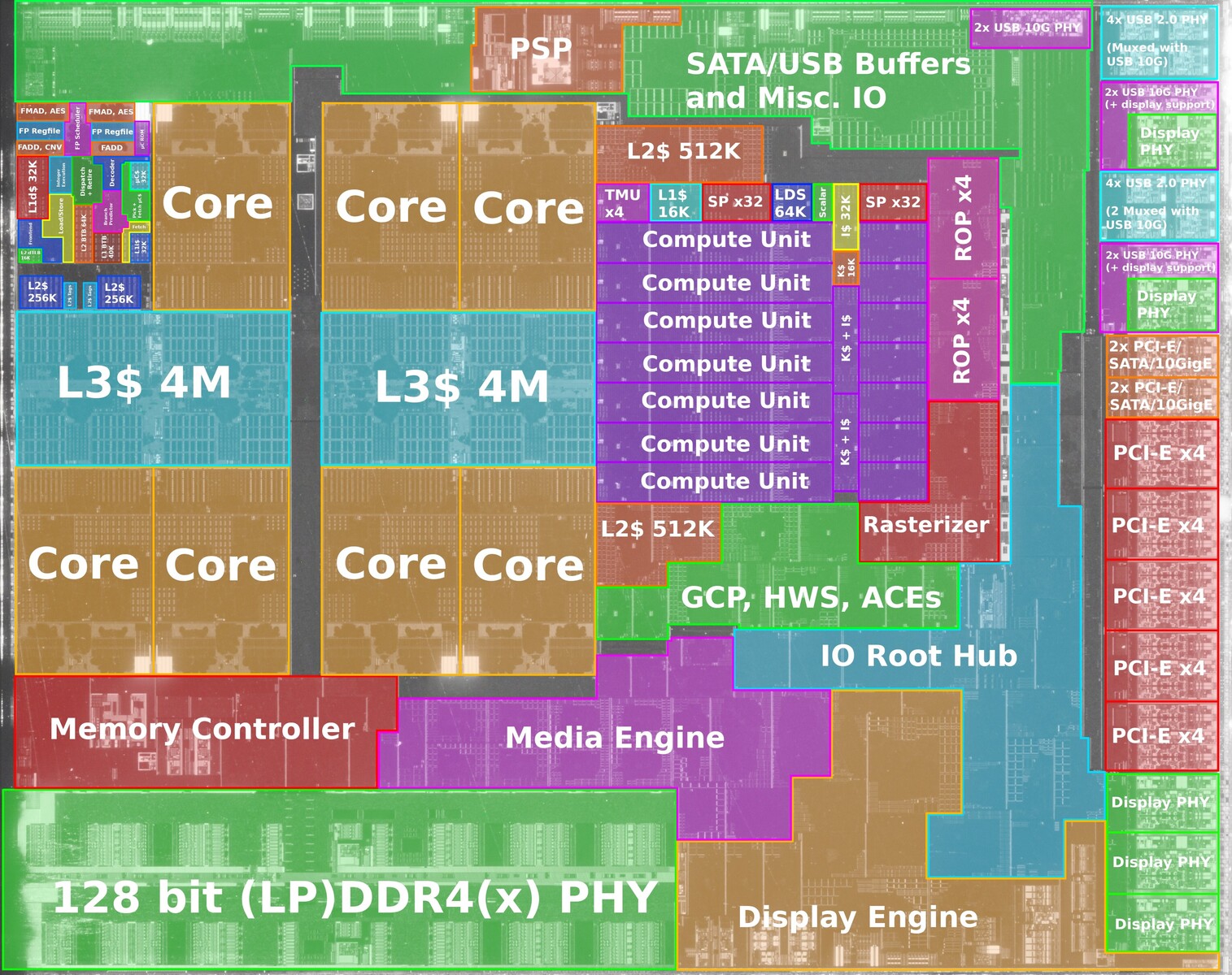
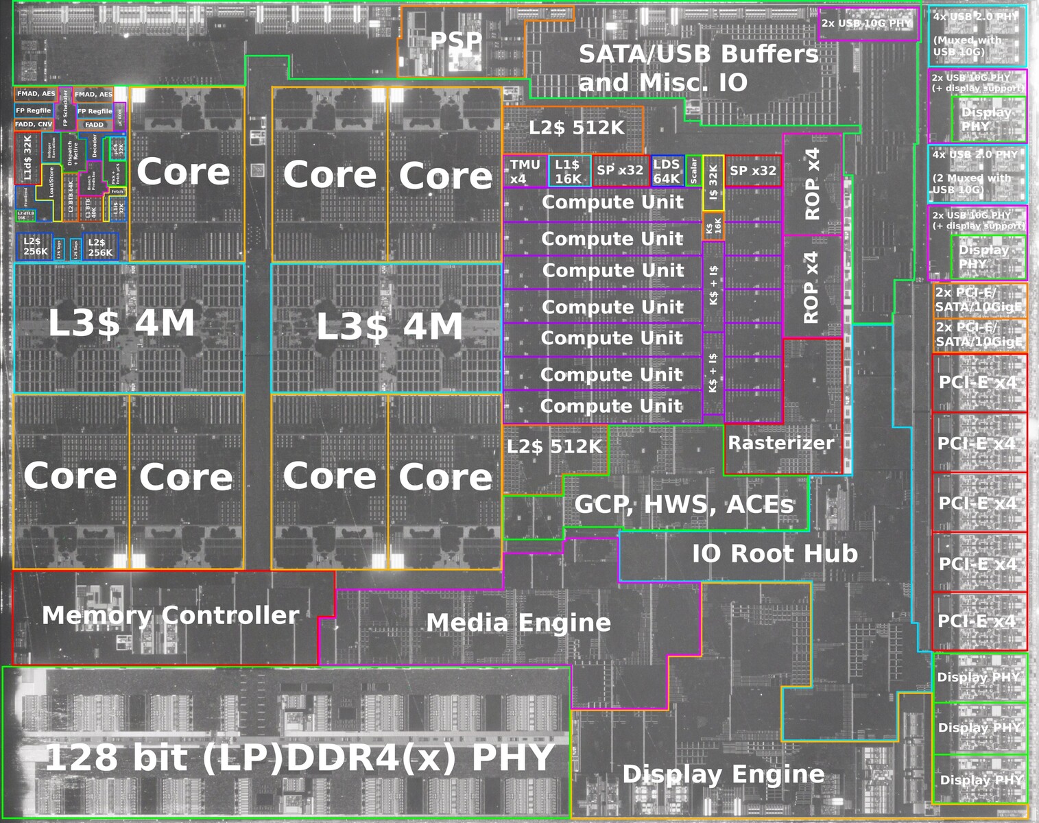
VLSI engineer Fritzchens Fritz, famous for high-detail EM photography of silicon dies and annotations of them, recently published his work on AMD's 7 nm "Renoir" APU silicon. His die-shots were annotated by Nemez aka GPUsAreMagic. The floor-plan of the silicon shows that the CPU component finally dwarfs the iGPU component, thanks to double the CPU cores over the previous-gen "Picasso" silicon, spread over two CCXs (compute complexes). The CCX on "Renoir" is visibly smaller than the one on the "Zen 2" CCDs found in "Matisse" and "Rome" MCMs, as the L3 cache is smaller, at 4 MB compared to 16 MB. Being MCMs with disintegrated memory controllers, it makes more sense for CCDs to have more last-level cache per CCX.
We also see that the iGPU features no more than 8 "Vega" NGCUs, so there's no scope for "Renoir" based desktop APUs to feature >512 stream processors. AMD attempted to compensate for the NGCU deficit by dialing up engine clocks of the iGPU by over 40% compared to those on "Picasso." What caught our eye in the annotation is the PCI-Express physical layer. Apparently the die indeed has 20 PCI-Express lanes besides an additional 4 lanes that can be configured as two SATA 6 Gbps ports thanks to SerDes flexibility.