Please note that this post is tagged as a rumor .
Update:
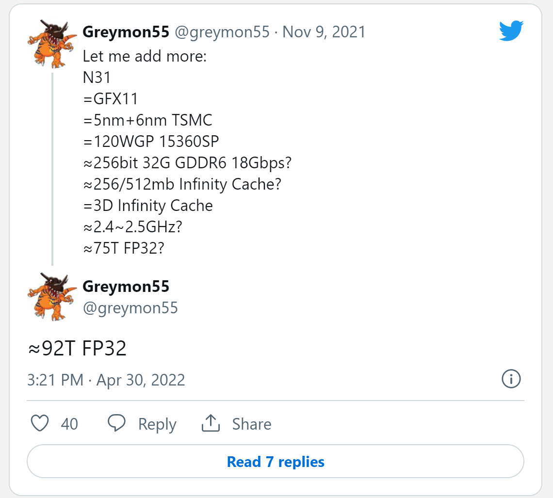
Greymon55 clarified that the 92 TFLOPS claim was referring to the old, rumored 15360 Stream Processor configuration. He has since provided an update now claiming that the core count is 12288 Stream Processors. This means that the card with 3 GHz clock would feature 73 TFLOPS, not 92 as he claimed.
AMD Radeon RX 7900XT could potentially feature 3 GHz GPU clock
AMD leaker Greymon55 provides an update to half a year rumors on Navi 31 GPU.

The leaker now claims that the GPU might hit 92 TFLOPS of FP32 performance, which is 28% more than the previous claim of 75 TFLOPS. This new number is also four times as high as RDNA2 based Navi 21 GPU (RX 6900XT) model.
Greymon55 earlier mentioned that there is a major change to the specs that were shared for more than a year, but has not explained what those changes are. However, should AMD keep 60 WorkGroup Processor (WGP) and 15360 Stream Processor configuration, such single-precision compute performance would require 2995 MHz GPU clock. However, it is very likely that similarly to NVIDIA and their Ada architecture, AMD will be introducing a matrix of different 32-bit instructions that result in higher floating point performance.
Furthermore, contrary to previous rumors, AMD might still keep Compute Units for its RDNA3 (GFX11) architecture. This is suggested by the recent changes to AMD GPU driver discovered by @Kepler_L2:
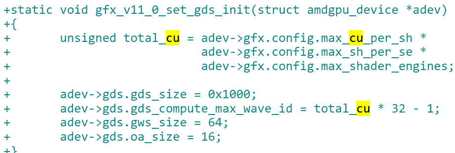
AMDGPU driver,Source: Freedesktop
AMD Radeon RX 7000 series are now expected to launch by the end of this year. The Navi 31 GPU should be among the first to be announced by AMD, most likely for RX 7900 XT class graphics card, the new flagship consumer SKU.
| Next-gen Flagship GPU Comparison (RUMORED) | |||
|---|---|---|---|
| VideoCardz.com | GeForce RTX 4090 – Class | Radeon RX 7900 – Class | Arc B9XX – Class |
| Fabrication Node | TSMC N5 | TSMC N5/N6 | TBC |
| Architecture | NVIDIA Ada | AMD RDNA3 | Intel Xe2-HPG “Battlemage” |
| GPU Package | Monolithic | Multi-Chip-Module (MCM) | Multi-Chip-Module (MCM) |
| Estimated GPU Size | ~600mm² | ~800mm² | TBC |
| Graphics Dies | 1 | 2 GCD + 4 MCD + 1 IOD | 4 Tiles |
| GPU Mega Clusters | 12 Graphics Processing Clusters (GPC) | 2×3 Shader Engines | 10 Render Slices |
| GPU Super Clusters | 72 Texture Processing Clusters (TPC) | 2×30 RDNA Workgroups (WGP) | 40 Xe-Cores |
| GPU Clusters | 144 Streaming Multiprocessors (SM) | 120 Compute Units | 1280 Xe Vector Engines |
| FP32 Cores | 18432 CUDA Cores | 15360 Stream Processors | 20480 FP32 ALUs |
| GPU Clock | ~ 2.7 GHz | ~ 3.0 GHz | TBC |
| Memory Type | 24 GB GDDR6X | TBC GB GDDR6 | TBC |
| Memory & Bus | 21 Gbps 384-bit | TBC Gbps 256-bit | TBC |
| Cache | 96MB (L2 Cache) | 256 or 512MB Infinity Cache | TBC |
| Power Consumption | 600W (TDP) | TBC | TBC |
| Release Date | Q3/Q4 2022 | Q3/Q4 2022 | 2023-2024 |
| Rumored Performance | ~ 100 TFLOPs FP32 * | ~ 92 TFLOPs FP32 | TBC |
* Updated as Greymon55 suggests FP32 performance of AD102 GPU could reach 100 TFLOPS.
Source: @Greymon_55 , @Kepler_L2