Please note that this post is tagged as a rumor .
AMD MI300 with up to 5nm Compute Dies
We are still in the early stage of next-gen AMD Instinct MI300 rumors, however Moore’s Law is Dead claims to have actual photos that were used to create the following renders of said GPUs.
Just as the MI200, the MI300 is a family of data-center GPUs. Therefore, one cannot say that MI300 has one set of specifications. On the contrary, the MI300 will be available in many formats, featuring from two to eight HBM3 memory stacks. Furthermore, the MI300 will feature 3D stacking with I/O (or base) chiplet right under the new compute dies.
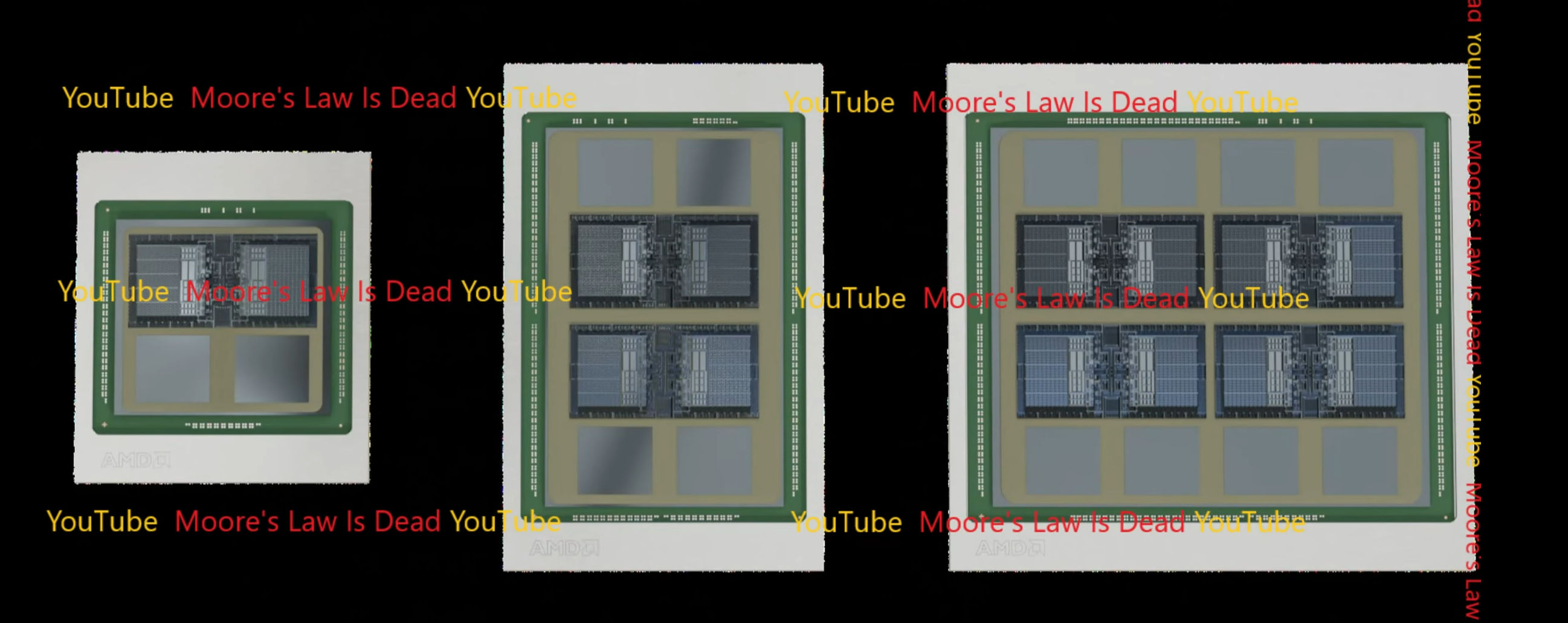
AMD MI300 GPU Family Render, Source: Moore’s Law is Dead
Here, one should note that Compute dies for MI300 will not supposedly feature a single type of IP block, but rather give customers some options to choose from. Under each 5nm Compute die, there is an I/O die. This base tile which is manufactured using 6 nm process is attached to two stacks of HBM3 memory. This would be the first time AMD is using 3D stacked dies.
In terms of power, each Compute die may consume around 150 Watts. So the top configuration could consume more than 600W, which shouldn’t really be that surprising considering MI250X already has 560W TDP spec for the OAM form factor.
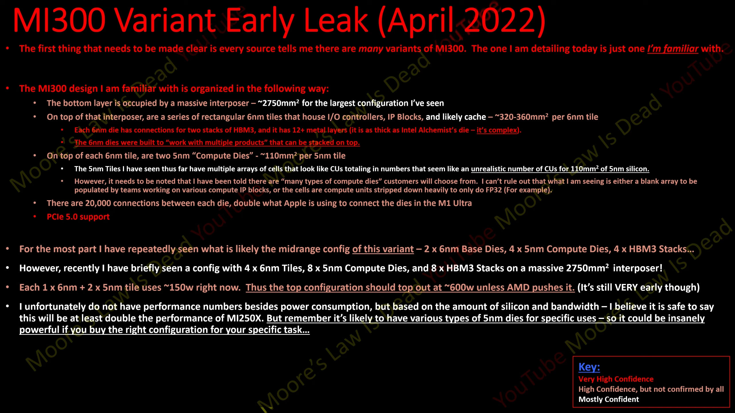
AMD MI300 GPU Rumors, Source: Moore’s Law is Dead
Each Compute Die should measure around 110 mm², while the interposer for the biggest variant would be as big as 2750 mm². These Compute dies would also have around 20,000 connections with each other, which is a double of what Apple offers for its M1 Ultra silicon compute chiplets.
The release date of Instinct MI300 is currently unknown, but there is a good reason to believe that by the time MI300 is released, NVIDIA Hopper and Intel Ponte Vecchio should already be available on the market.
| RUMORED AMD Instinct Accelerators Specifications | ||||
|---|---|---|---|---|
| VideoCardz | AMD Radeon Instinct MI60 | AMD Instinct MI100 | AMD Instinct MI250X | AMD Instinct MI300 (flagship) |
| Architecture & Nodes | 7nm GCN5 (GFX906) | 7nm CDNA1 (GFX908) | 6nm CDNA2 (GFX90A) | 5nm CDNA3 (GFX940) + 6nm (base) |
| GPU | Vega 20 | Arcturus | Aldebaran (MCM) | ? (3D Die Stacking) |
| Base Chiplets | – | – | – | 2 |
| Compute Tiles | 1 | 1 | 2 | 8 |
| Compute Units | 64 | 120 | 220 | TBC |
| GPU Clock Speed | 1800 MHz | ~1500 MHz | ~1700 MHz | TBC |
| FP16 Compute | 29.5 TFLOPS | 185 TFLOPS | 383 TFLOPS | TBC |
| FP32 Compute | 14.7 TFLOPS | 23.1 TFLOPS | 47.9 TFLOPS | TBC |
| FP64 Compute | 7.4 TFLOPS | 11.5 TFLOPS | 47.9 TFLOPS | TBC |
| VRAM | 32 GB HBM2 | 32 GB HBM2 | 128 GB 8x HBM2e | 8x HBM3 stack |
| Memory Clock | 2.0 Gbps | 2.4 Gbps | 3.2 Gbps | TBC |
| Memory Bus | 4096-bit | 4096-bit | 8192-bit | 8192-bit |
| Memory Bandwidth | 1 TB/s | 1.23 TB/s | 3.2 TB/s | TBC |
| Form Factor | Dual Slot, Full Length | Dual Slot, Full Length | OAM | OAM |
| TDP | 300W | 300W | 560W | 600W+ |
Source: