Please note that this post is tagged as a rumor .
AMD flagship RDNA3 GPU reportedly has a small graphics die, but there is a reason
The upcoming Navi 31 GPU reportedly features 350 mm² graphics die, significantly smaller than the rumored figures from last year.
According to Greymon55, AMD Navi 31 GCD (Graphics Complex Die) is only 350 mm² in size. That’s a relatively small die compared to existing Navi 21 GPU (520 mm²), but the design of next-gen AMD RDNA3 architecture is not as straightforward to simply be compared to current-gen GPUs.
The following mockup shows rumored GCD size relative to Navi 21 GPU die. Do note that package size or MCD size is still unknown.
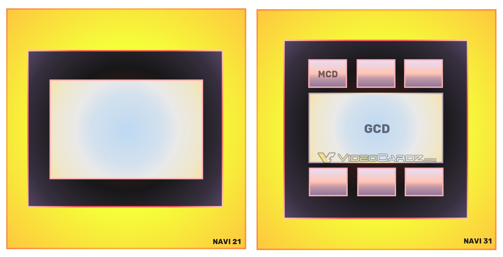
Estimated Navi 31 GCD size compared to Navi 21 GPU, Source: VideoCardz
AMD RDNA3 architecture is to feature advanced packaging technology with GCD and MCD (Memory Complex Die) connected to each other. The Navi 31 GPU is said to feature one GCD and up to six MCDs. The innovative GCD+MCD design is to be used by both Navi 31 and Navi 32 GPUs, with Navi 33 going the monolithic way. With an estimated GCD size of 350 mm², and six GCDs at 40 mm² each, the full design could measure 590 mm² which is almost as big as the rumored NVIDIA AD102 GPU (~600 mm²).
GCD 350mm²+
— Greymon55 (@greymon55) July 19, 2022
As pointed out by 3DCenter.org , the AMD Navi 21 GPU without the Infinity Cache and memory controllers (things that should end up in MCDs), would be 375 mm² in size, so still larger than the rumored Navi 31 figure.
But there is a reason why Navi 31’s GCD is relatively smaller. As noted by @Kepler_L2 who has been analyzing the AMD RDNA3 Linux updates, the new architecture will remove some unnecessary graphics complex from RDNA3 die: XGMI, Global Data Share (GDS), Legacy Geometry Pipeline or Legacy Scan Converter. Those things combined with a smaller process node may explain the size of Navi 31 GCD.
One should also mention that Greymon55 has already teased a possibility of AMD releasing an even more advanced GPU. This mysterious chip is reportedly designed for 16384 core count, which should be expected later. Very little is known about this GPU otherwise, and it is not entirely clear if it will make its way to the consumer space in the first place. However, given NVIDIA’s aggressive and power-hungry plans for Ada GPUs, this new chip may be exactly what AMD needs to compete.
| RUMORED Specs of AMD RDNA3 GPUs | ||||
|---|---|---|---|---|
| VideoCardz.com | AMD NAVI 3X | AMD NAVI 31 | AMD NAVI 32 | AMD NAVI 33 |
| Fabrication Node | TBC | TSMC 5nm + 6nm | TSMC 5nm + 6nm | TSMC 6nm |
| Architecture | AMD RDNA3 | AMD RDNA3 | AMD RDNA3 | AMD RDNA3 |
| GPU Package | Multi-Chip-Module (MCM) | Multi-Chip-Module (MCM) | Multi-Chip-Module (MCM) | Monolithic |
| GPU Size | TBC | 1x 350 + 6x 40 ≈ 590 mm² | TBC | TBC |
| Configuration | 2x GCD + (?) MCD | 1x GCD + 6x MCD | 1x GCD + 4x MCD | TBC |
| Shader Engines | 8 | 6 | 4 | 2 |
| Shader Arrays | 16 | 12 | 8 | 4 |
| RDNA Workgroups (WGP) | 64 | 48 | 32 | 16 |
| Compute Units | 128 | 96 | 64 | 32 |
| Stream Processors | 16384 | 12288 | 8192 | 4096 |
| Memory & Bus | TBC | 24GB GDDR6 384-bit | 16GB GDDR6 256-bit | 8GB GDDR6 128-bit |
| Memory Bandwidth | TBC | 864 GB/s (18 Gbps) | 576 GB/s (18 Gbps) | 288 GB/s (18 Gbps) |
| Infinity Cache | TBC | 192 MB | 128 MB | 64 MB |
| PCIe Interface | TBC | PCIe Gen5 | PCIe Gen5 | PCIe Gen5 |
| Release | 2023 | Q3 2022 | Q1 2023 | Q4 2022 |
| Rumored SKU | Radeon PRO | Radeon RX 7900XT | Radeon RX 7700XT | Radeon RX 7600XT |
| All information based on rumors. (Updated: July 20 2022) |
Source: @Greymon55