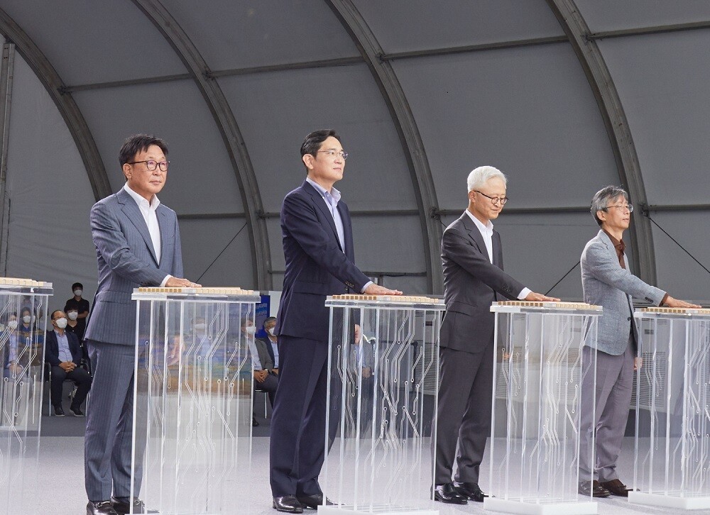
Samsung Electronics today broke ground for a new semiconductor research and development complex in Giheung, Korea, aiming to extend its leadership in state-of-the-art semiconductor technology. Samsung Electronics plans to invest about KRW 20 trillion by 2028 for the complex in an area covering about 109,000 square meters within its Giheung campus. The new facility will lead advanced research on next-generation devices and processes for memory and system semiconductors, as well as development of innovative new technologies based on a long-term roadmap.
Today's groundbreaking ceremony was attended by Samsung Electronics Vice Chairman Jay Y. Lee, President and CEO Kye Hyun Kyung, President of the Memory Business Jung-Bae Lee, President of the Foundry Business Siyoung Choi and President of the S.LSI Business Yong-In Park, along with more than 100 employees.