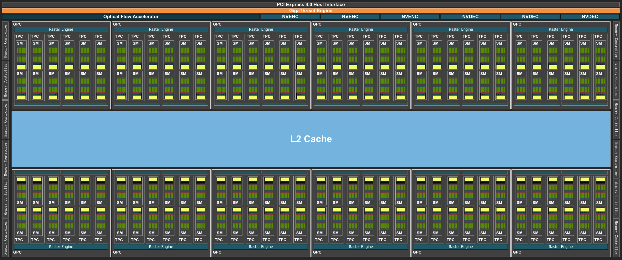
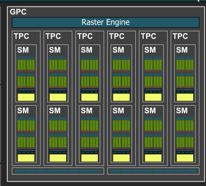
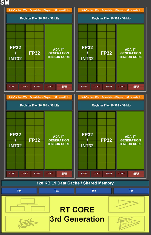
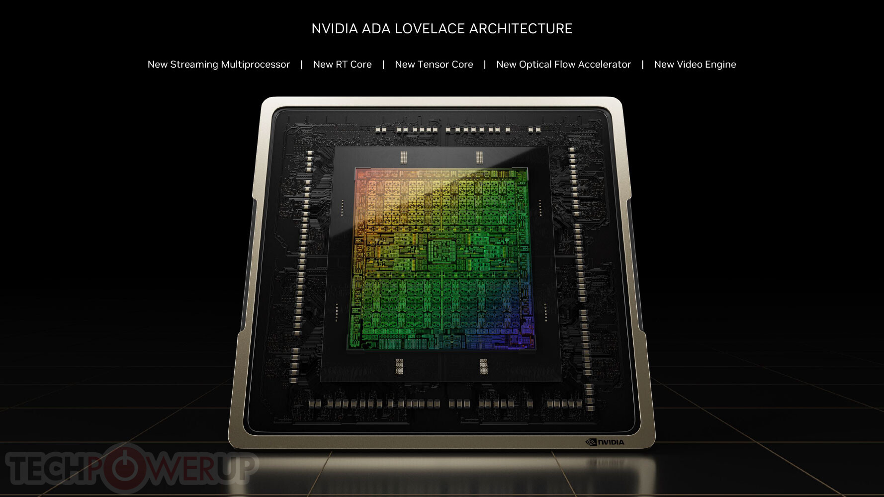
At the heart of the GeForce RTX 4090 is the gigantic AD102 silicon, which we broadly detailed in an older article. Built on the 4 nm silicon fabrication process, this chip measures 608 mm² in die-area, and crams in 76.3 billion transistors. We now have our first look into the silicon-level block diagram of the AD102, including the introduction of several new components.
The AD102 features a PCI-Express 4.0 x16 host interface, and a 384-bit GDDR6X memory interface. The Gigathread Engine acts as a the main resource allocation component of the silicon. Ada introduces the Optical Flow Accelerator, a component crucial for DLSS 3 to generate entire frames without involving the graphics rendering machinery. The chip features double the number of media-encoding hardware engines as "Ampere," including hardware-accelerated AV1 encode/decode. Multiple accelerators mean that multiple streams of videos can be transcoded (helpful in a media production environment).