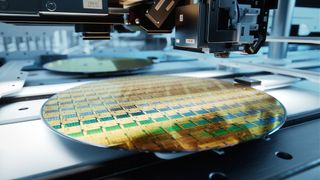
TSMC will reportedly hike the pricing of wafers processed using its leading edge N3 (3nm-class) process technology by 25% compared to N5 (5nm class) production node. This will immediately make complex processors like GPUs and smartphone SoCs more expensive, which will make devices like graphics cards and handsets costlier. Meanwhile, prohibitively high costs will make multi-chiplet designs more appealing.
One wafer processed on TSMC's leading edge N3 manufacturing technology will cost over $20,000 according to DigiTimes (via @RetiredEngineer ). By contrast, an N5 wafer costs around $16,000, the report says.
There are many reasons why making chips on N5 and N3 production nodes is expensive. First up, both technologies use extreme ultraviolet (EUV) lithography pretty extensively for up to 14 layers in N5 and even more with N3. Each EUV tool costs $150 million, and multiple EUV scanners have to be installed in a fab, which means additional costs for TSMC. Also, it takes a long time to produce chips on N5 and N3, which again means higher costs for TSMC.
TSMC's Alleged Wafer Pricing
TSMC doesn't generally reveal prices for its wafers, except to actual customers. It's also important to note that contract pricing — what larger orders from companies like Apple, AMD, Nvidia, and even rival Intel are likely to use — may be lower than the base prices. Still, here's what the report says about current prices.
| Price per Wafer | $20,000 | $16,000 | $10,000 | $6,000 | $3,000 | $2,600 | $2,000 |
| Node | N3 | N5 | N7 | N10 | N28 | 40nm | 90nm |
| Year | 2022 | 2020 | 2018 | 2016 | 2014 | 2008 | 2004 |
Chip developers who use TSMC's services are expected to pass the costs of new chips on to downstream customers, which will make smartphones and graphics cards more expensive. Even now, Apple's iPhone 14 Pro starts at $999, whereas Nvidia's flagship GeForce RTX 4090 is priced at $1,599. Once companies like Apple and Nvidia adopt TSMC's N3 node, we can expect their products to get even more expensive.
Of course the actual chip cost can still be relatively small compared to all the other parts that go into a modern smartphone or graphics card. Take Nvidia's AD102, which measures 608mm^2. Dies per wafer calculators estimate Nvidia can get about 90 chips from an N5 wafer, or a base cost of $178 per chip. Packaging, PCB costs, components, cooling, etc. all contribute probably at least twice that much, but the real cost is in the R&D aspects of modern chip design.
| Header Cell - Column 0 | N3E vs N5 | N3 vs N5 |
|---|---|---|
| Speed Improvement @ Same Power | +18% | +10% ~ 15% |
| Power Reduction @ Same Speed | -34% | -25% ~ -30% |
| Logic Density | 1.7x | 1.6x |
| HVM Start | Q2/Q3 2023 | H2 2022 |
While there are rational reasons why TSMC's prices are getting higher, it should be noted that that the company can get away with it as it currently doesn't have any rivals that can produce chips using a leading edge fabrication technologies with decent yields and in high volumes. While formally Samsung Foundry is ahead of TSMC with its 3GAE process technology (3nm-class, gate all around transistors), it is believed that it is used only for tiny cryptocurrency mining chips due to insufficient yields. Meanwhile, Samsung Foundry's 4nm-class process technology did not live up to expectations as far as performance is concerned.
When (and if) Samsung and Intel Foundry Services offer process technologies that outperform those of TSMC, the world's largest foundry will have to somewhat limit its prices, although we do not expect chip prices to drop because of intensified competition on the foundry market as fabs are getting more expensive, chip development costs are rising, and fabrication technologies are getting more complex.
In general, the costs of making chips on leading edge nodes began to rise rapidly in mid-2010s when Intel, GlobalFoundries, Samsung, TSMC, and UMC adopted FinFET transistors. At the time costs rose for everyone despite intense competition between contract semiconductor manufacturers.
TSMC's first client to use N3 is expected to be Apple, which can afford developing an appropriate SoC, produce it in high volume, and still make money on its hardware. Apple has not indicated what kind of processors the company plans to make on N3, but a follow-up to the current M2 and A16 Bionic seems logical. Other chip developers may hold off using TSMC's N3 for now because of its prohibitively high costs and use chiplet-based designs instead due to lower development costs, lower risks, and lower production costs.
Again, please note that TSMC does not comment on its quotes and has not commented on information that it will charge ~$20,000 per N3 wafer. Those figures come from industry insiders and may or may not reflect actual high volume prices.