A more detailed look at the architecture has been provided by NVIDIA. The company released block diagrams, technology descriptions and detailed specifications.
NVIDIA details Ampere architecture
NVIDIA has confirmed the expected performance figures for its new Ampere models. These are official figures based on NVIDIA in-house benchmarks, likely to be taken with a grain of salt. However, they show what the company expects from the current stack and how should it be placed for future comparisons.
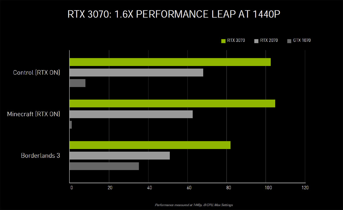
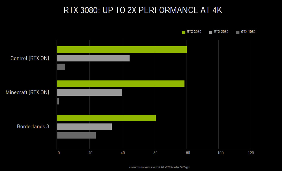
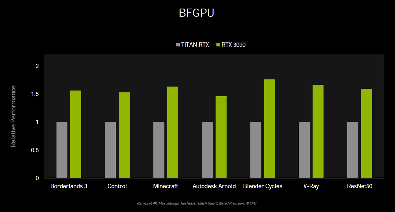
Official NVIDIA RTX 30 Performance (according to NVIDIA)
NVIDIA also revealed detailed specs of the Ampere GPUs. The GPUs build using the Samsung 8nm node have a transistor destiny of 44.6MT/mm 2 (GA102) compared to 24.7 MT/mm 2 for Turing (TU102). The biggest Ampere RTX GPU – GA102 has 28 billion transistors and a die size of 628.4 mm 2 . This GPU will be used for GeForce RTX 3090 and RTX 3080. The flagship model features 82 Streaming Multiprocessors with 328 Tensor cores and 82 RT cores (ray tracing cores). It also has a 384-bit memory bus and 6MB of L2 cache.
A smaller Ampere GPU, GA104, features 17.4 billion transistors and a die size of 692.5 mm 2 . The RTX 3070 graphics card has 46 SMs enabled and thus the number of Tensors is 184 and RT cores is 46. This GPU has a memory bus of 256-bit and 4MB of L2 cache.
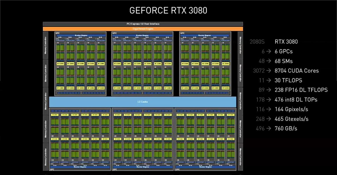
NVIDIA RTX 3080 (GA102) Block Diagram
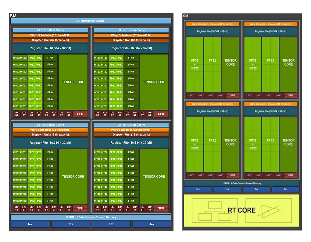
NVIDIA Ampere Streaming Multiprocessor
| NVIDIA GeForce RTX 30 Series Specifications | ||||
|---|---|---|---|---|
| VideoCardz.com | RTX 3090 | RTX 3080 | RTX 3070 | RTX 2080 Ti |
| Picture | 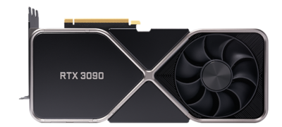 | 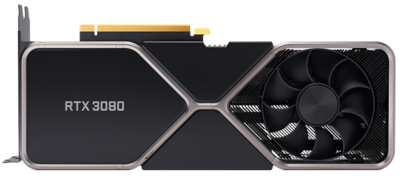 | 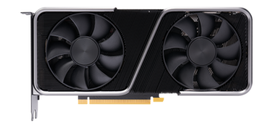 | 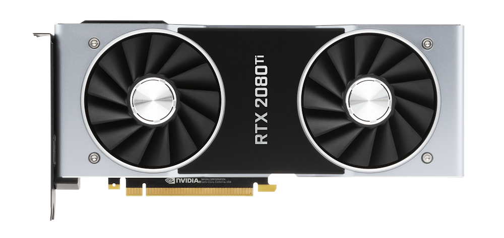 |
| GPU | 8nm GA102-300 | 8nm GA102-200 | 8nm GA104-300 | 12nm TU102-300 |
| Die Size | 628 mm2 | 628 mm2 | 392 mm2 | 754 mm2 |
| Transistors | 28 B | 28 B | 17.4 B | 18.6 B |
| Board | PG132 SKU 30 | PG132 SKU 10 | PG142 SKU 10 | PG150 SKU 32 |
| CUDA Cores | 10496 | 8704 | 5888 | 4352 |
| Tensor Cores | 328 (4 per SM) | 272 (4 per SM) | 184 (4 per SM) | 544 (8 per SM) |
| RT Cores | 82 | 68 | 46 | 68 |
| Base Clock | 1395 MHz | 1440 MHz | 1500 MHz | 1350 MHz |
| Boost Clock | 1695 MHz | 1710 MHz | 1725 MHz | 1545 MHz |
| Shader Perf. | 35.6 TFLOPS | 29.8 TFLOPS | 20.3 TFLOPS | 13.4 TFLOPS |
| RT Perf. | 285 TFLOPS | 283 TFLOPS | 163 TFLOPS | 110 TFLOPS |
| Memory | 24GB G6X | 10GB G6X | 8GB G6 | 11GB G6 |
| Memory Clock | 19.5 Gbps | 19 Gbps | 14 Gbps | 14 Gbps |
| Memory Bus | 384-bit | 320-bit | 256-bit | 352-bit |
| Bandwidth | 936 GB/s | 760 GB/s | 441 GB/s | 616 GB/s |
| TDP | 350W | 320W | 220W | 250W |
| MSRP | $1499 | $699 | $499 | $999 |
RT Cores
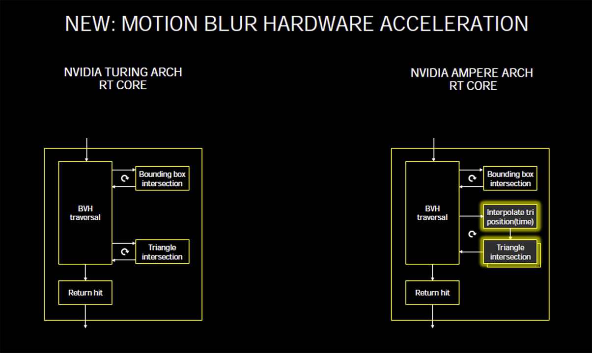
NVIDIA GeForce RTX 30 series introduces Second Generation RT cores, improving ray tracing acceleration. NVIDIA RT cores have pure hardware-based bounding volume hierarchy (BVH) which greatly improves performance over traditional and minimalistic approach with SIMD stream processors.
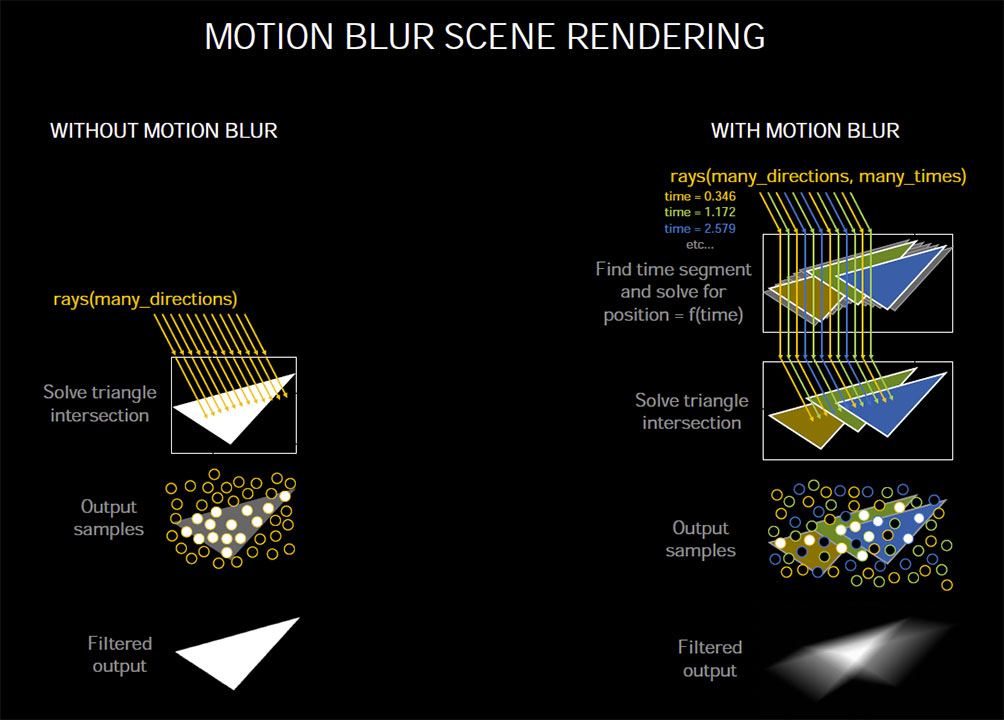
The second-generation Ampere RT core adds a triangle interpolation component along a time-scale, in coordination with the triangle intersection unit to the RT core architecture.
According to NVIDIA, this should be useful during motion blur effects in real-time ray tracing.

Tensor Cores
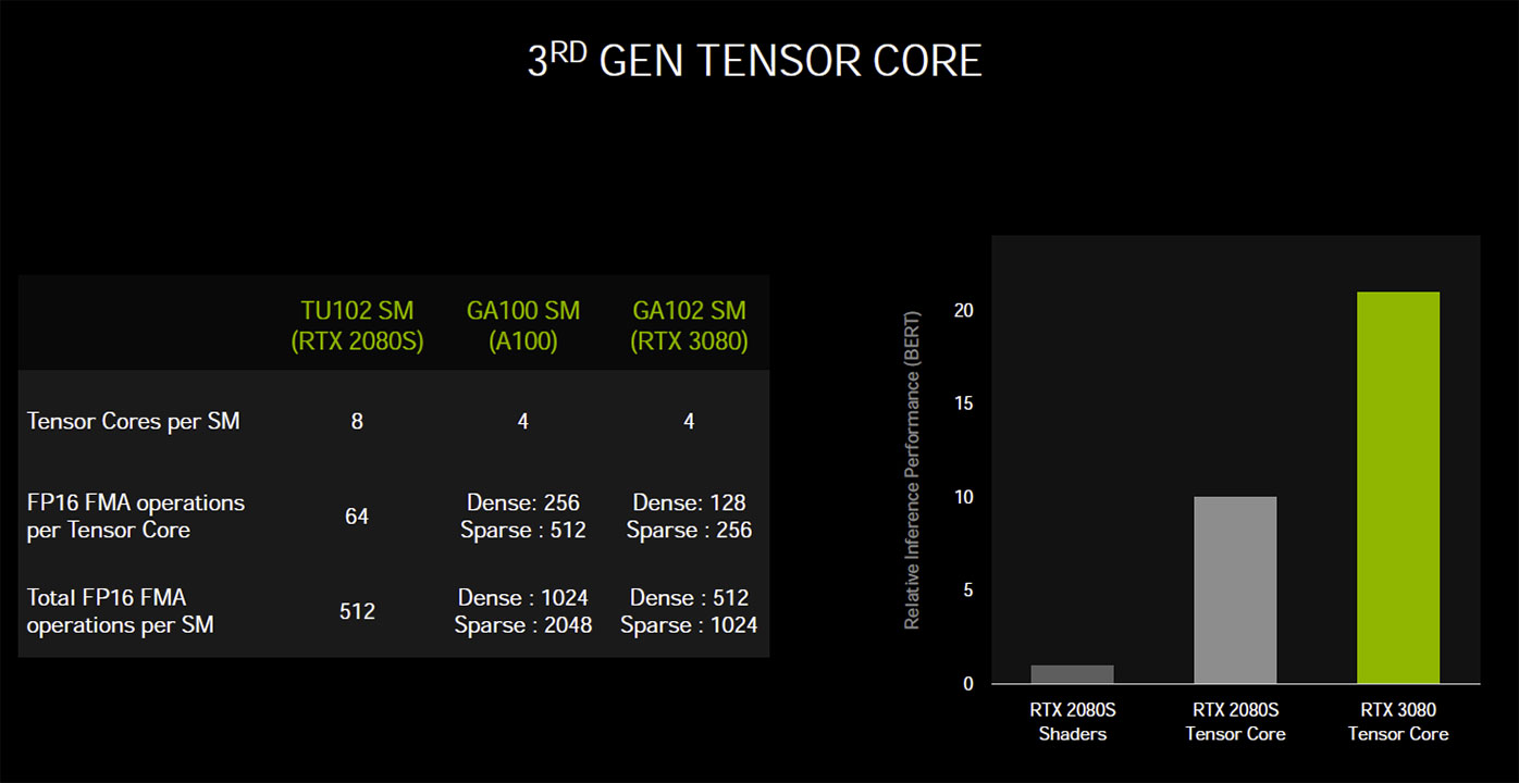
A third-generation Tensor core largely copies the design from (formerly Tesla) A100 Accelerator. This core will boost the performance during DLSS AI-super resolution upscaling in gaming.
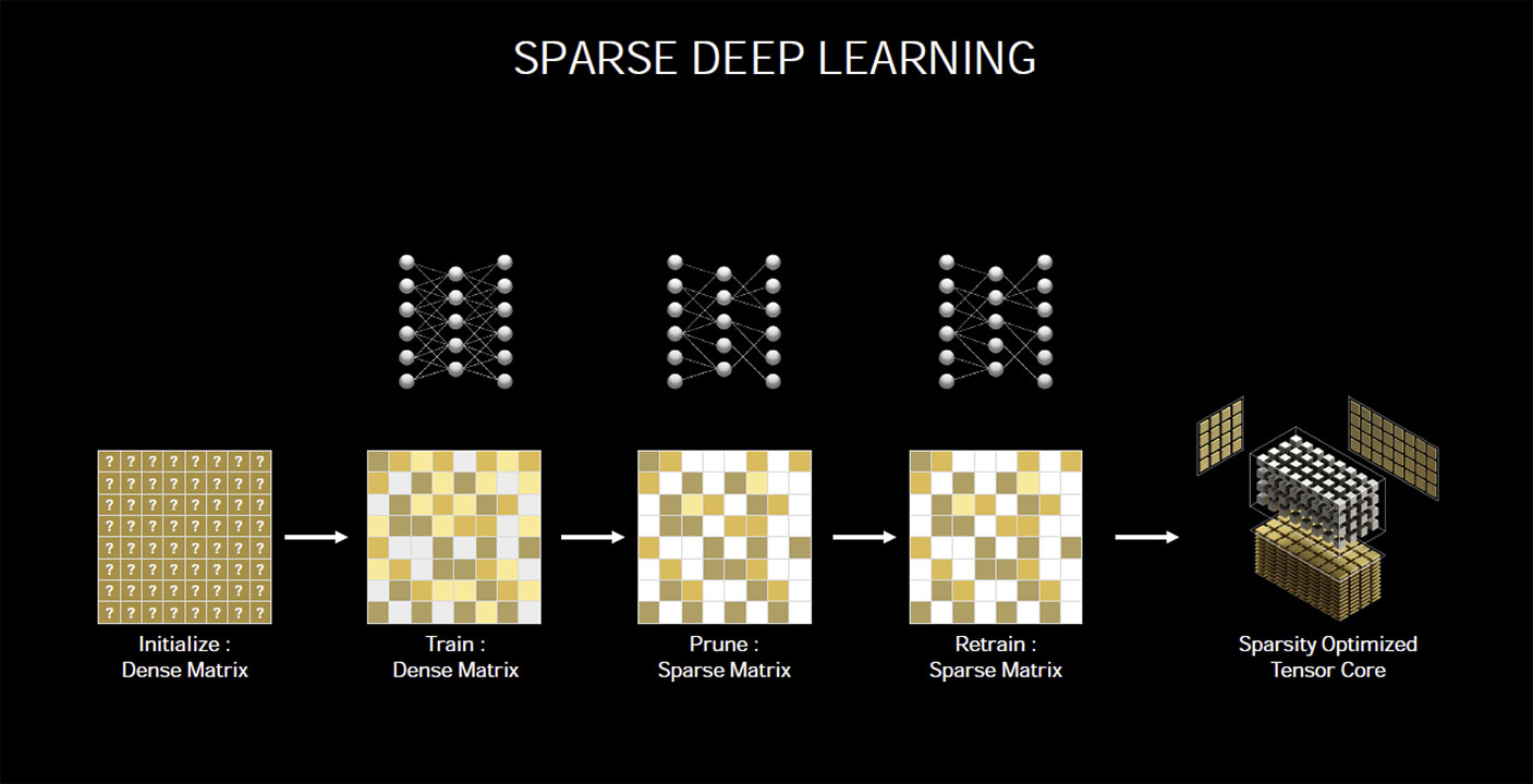
Ampere’s tensors are designed to leverage sparsity in deep learning neural nets. This is a process of reducing the matrixes without affecting its accuracy. This process can improve AI performance by an order of magnitude.
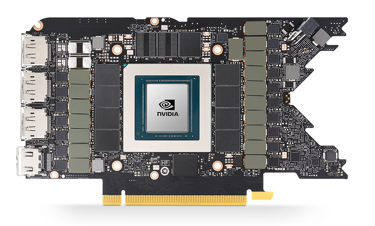
NVIDIA GA102 PCB
NVIDIA released a first official picture of the GA102-based Founders Edition graphics card featuring a PCI-Express 4.0 connector. This particular board design is for the GeForce RTX 3080. Unlike the RTX 3090, this board design has two missing memory modules and it lacks the NVLink connector (which is exclusive to RTX 3090 models).
A total of 12 GDDR6X modules can be mounted on this board, but the RTX 3080 only has 10.
The PCB features 20-phase VRM which are put on both sides of the GPU. The DrMOS and tantalum capacitors were mostly put on the rear of the board.
The RTX 30 series biggest innovations is the new Molex Microfit 12-pin power connector, capable of delivering up to 300W of power. NVIDIA will not restrict Intel or AMD from using this connector, so there is a change that we see an adoption of the new standard pretty soon.
Source: TechPowerUP , HotHardware