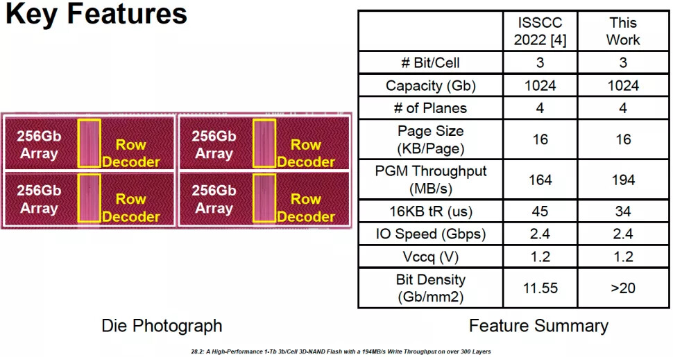
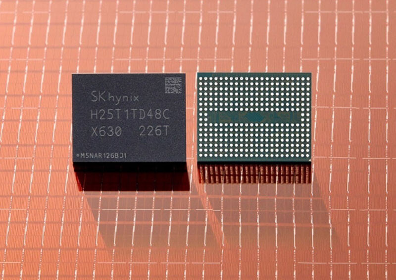
SK Hynix representatives unveiled the company's latest breakthrough in 3D NAND development at the ISSCC 2023 conference. Details of a new flash memory prototype featuring over 300 layers were revealed, and the company stated that a team of 35 engineers had contributed to the presentation material. In order to highlight the boost in performance offered by the prototype's improvements, it was compared to SK Hynix's previous record holding seventh-generation 238-layer 3D NAND. The new eighth-generation 3D NAND posted bandwidth figures with a maximum of 194 MB/s, which contrasts favorably with the older model's rate of 164 MB/s, representing an 18% increase in performance.
Recording density also benefits from the 300+ active layer design, with SK Hynix mentioning a 1 TB (128 GB) capacity with triple level cells and a bit density of over 20 GB/mm^2. The chip features a 16 KB page size, four planes and a 2400 MT/s interface. The increase in density will result in a lower per-TB cost during the manufacturing process. It is hoped that the end consumer will ultimately benefit from the boost in performance and capacity.