AMD launched its Instinct MI300X AI accelerator and the Instinct MI300A, the world’s first data center APU, during its Advancing AI event here in San Jose, California, as it looks to capitalize on the booming generative AI and HPC market. AMD forged its MI300 lineup using the most advanced production technologies ever pressed into mass production, employing new techniques like its ‘3.5D’ packaging to produce two multi-chip behemoths that it says provide Nvidia-beating performance in a wide range of AI workloads. AMD isn’t sharing pricing for its new exotic silicon, but the products are now shipping to a wide range of OEM partners.
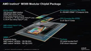
The Instinct MI300 is a game-changing design - the data center APU blends a total of 13 chiplets, many of them 3D-stacked, to create a chip with twenty-four Zen 4 CPU cores fused with a CDNA 3 graphics engine and 8 stacks of HBM3. Overall, the chip weighs in with 146 billion transistors, making it the largest chip AMD has pressed into production.
AMD says its Instinct MI300X GPU delivers up to 1.6X more performance than the Nidia H100 in AI inference workloads and offers similar performance in training work, thus providing the industry with a sorely needed high-performance alternative to Nvidia’s GPUs. Additionally, these accelerators come with more than twice the HBM3 memory capacity than Nvidia’s GPUs — an incredible 192 GB apiece — enabling its MI300X platforms to support more than twice the number of LLMs per system as well as running larger models than Nvidia’s H100 HGX.
The AMD Instinct MI300A builds on the same design as the MI300X but mixes CPU cores into the design while culling some of the GPU cores. AMD claims this chip delivers up to 4X more performance than Nvidia’s H100 GPUs in some workloads and touts that it has twice the performance per watt.
AMD Instinct MI300X
The MI300X represents the pinnacle of AMD’s chiplet-based design methodology, melding eight 12Hi stacks of HBM3 memory with eight 3D-stacked 5nm CDNA 3 GPU chiplets, dubbed XCD’s, on four underlying 6nm I/O dies that are connected using AMD’s now-mature hybrid bonding technique.

The result is a 750W accelerator that wields 304 compute units, 192GB of HBM3 capacity, and 5.3 TB/s of bandwidth. The accelerator also has 256MB of Infinity Cache that serves as a shared L3 cache layer to facilitate communication between the chiplets. AMD dubs its packaging tech that binds the chiplets together as ‘3.5D,’ denoting a combination of 3D-stacked GPU and I/O dies with hybrid bonding paired with standard 2.5D packaging for the remainder of the module. We’ll dive much deeper into the architectural components below.
The MI300X accelerator is designed to work in groups of eight in AMD’s generative AI platform, facilitated by 896 GB/s of throughput between the GPUs across an Infinity Fabric interconnect. This system has 1.5TB of total HBM3 memory and delivers up to 10.4 Petaflops of performance (BF16/FP16).
AMD’s MI300X platform has 2.4X more memory capacity and a claimed 1.3X advantage in computational horsepower over Nvidia’s H100 HGX platform (BF16/FP16), all while maintaining comparable aggregate bi-directional and single-node ring bandwidth. AMD outfits the MI300X platform with 400GbE networking and supports a wide variety of NICs, whereas Nvidia favors using its own networking products borne of its Mellanox acquisition.
As always, we should approach vendor benchmarks with caution. AMD shared a host of performance metrics, showing that it has up to 2.4X the peak theoretical FP64 and FP32 vector matrix throughput of the H100 for HPC workloads, and up to 1.3X higher peak theoretical TF32, FP16, BF16, FP8 and INT8 throughput for AI workloads, all projected without sparsity (the MI300X does support sparsity, though).
The MI300X’s hefty memory capacity and bandwidth is ideal for inferencing. AMD used a 176-billion-parameter Flash Attention 2 model to claim a 1.6X performance advantage over the Nvidia H100 in tokens/s throughput, and a 70-billion-parameter Llama 2 model to highlight a 1.4X chat latency advantage (measured from the start to the end of the 2K sequence length/128 tokens workload).
AMD’s MI300X platform delivered roughly the same amount of performance in a 30-billion-paramteer MPT training workload as the H100 HGX system, but it is important to note that this test isn’t a one-to-one comparison of accelerators. Instead, this test pits groups of eight accelerators against one another, so platform-level capabilities become more of a limiting factor.
Speaking of which, AMD also claims the MI300X platform’s memory capacity advantage allows hosting up to twice the number of 30B-parameter training models and 70B-parameter inference models than the H100 system. Additionally, the MI300X platform can support up to 70B training and 290B-parameter inference models, both of which are twice as large as the models supported by the H100 HGX.
Naturally, Nvidia’s forthcoming H200 GPUs will be more competitive on the memory capacity and bandwidth front, while compute performance will remain similar. Nvidia won’t start shipping those until next year, so the competitive comparison with the MI300X is still off on the horizon.
AMD Instinct MI300A
The AMD Instinct MI300A is the world’s first data center APU, meaning that it combines both a CPU and GPU in the same package, and it will compete directly with Nvidia’s Grace Hopper superchips, which have a CPU and GPU in separate chip packages that work in tandem. The MI300A has already scored a notable win in the El Capitan supercomputer , and AMD is shipping this silicon to its partners.
The MI300A uses the same fundamental design and methodology as the MI300X but substitutes in three 5nm core compute die (CCD) with eight Zen 4 CPU cores apiece, the same as found on the EPYC and Ryzen processors, thus displacing two of the XCD GPU chiplets.
That leaves the MI300A armed with 24 threaded CPU cores and 228 CDNA 3 compute units spread across six XCD GPU chiplets. As with the MI300X, all the compute chiplets are hybrid bonded to four underlying I/O Dies (IOD) to enable far superior bandwidth, latency, and energy efficiency than standard chip-packaging techniques can achieve.
AMD culled the memory capacity by using eight 8Hi HBM3 stacks instead of the eight 12Hi stacks used for the MI300X, thus cutting capacity from 192GB to 128GB. However, memory bandwidth remains at 5.3 TB/s. AMD tells us the decision to reduce the memory capacity wasn’t due to power or thermal limitations; instead, it tailors the chip for the targeted HPC and AI workloads. Regardless, the 128GB of capacity and 5.3 TB/s of throughput are both still 1.6X more than provided by Nvidia’s H100 SXM GPU.
The MI300A has a default 350W TDP, but it is configurable up to 760W. AMD dynamically allocates power between the CPU and GPU portions of the chip based upon usage, thus optimizing performance and efficiency.
The memory space is shared between the CPU and GPU, thus eliminating data transfers. This technique boosts performance and energy efficiency by eliminating data transfers between the units, while also reducing the coding burden. As with the MI300X, the chip has a central 256MB Infinity Cache that helps ensure bandwidth and latency for data flowing through the chip.
AMD claims a 1.8X advantage over the H100 in FP64 Matrix/DGEMM and FP64/FP32 Vector TFLOPS. The company also claims parity with the H100 in TF32, FP16, BF16, FP8, and INT8.
AMD claims its MI300A is 4X faster than Nvidia’s H100 in an OpenFOAM HPC motorbike test, but this comparison isn’t ideal: The H100 is a GPU, while the blended CPU and GPU compute in the MI300A provides an inherent advantage in this memory-intensive workload through its shared memory addressing space. Comparisons to the Nvidia Grace Hopper GH200 Superchip, which also brings a CPU and GPU together in a tightly coupled implementation, would be better here, but AMD says that it couldn’t find any publicly listed OpenFOAM results for Nvidia’s chip.
AMD did present comparative perf-per-watt data to Nvidia’s GH200 to highlight a 2X advantage, with these results based on publicly available information about the H200. AMD also highlighted comparisons to the H100 in the Mini-Nbody, HPCG, and Gromacs benchmarks, claiming leads of 1.2X, 1.1X, and 1.1X, respectively. Again, comparisons to the GH200 would be more ideal for this set of benchmarks.
AMD Instinct MI300X and MI300A Architecture
We covered the basics of the design above, and those details provide important perspective to understand the sections below.
AMD leverages TSMC’s 3D hybrid bonding SoIC (silicon-on-integrated-circuit) tech to 3D-stack the various compute elements, be they the CPU CCDs (core compute die) or the GPU XCDs, atop the four underlying I/O Dies. Each I/O Die can house either two XCDs or three CCDs. Each CCD is identical to the existing EPYC chips, holding eight hyperthreaded Zen 4 cores apiece. Three of these CCDs and six XCDs are used to create the MI300A, while the MI300X uses eight XCDs.
The HBM stacks are connected using a standard interposer with 2.5D packaging technology. AMD’s combination of 2.5D and 3D packaging techniques led the company to coin the ‘3.5D’ packaging moniker. Each I/O die houses a 32-channel HBM3 memory controller to host two of the eight HBM stacks, resulting in 128 total 16-bit memory channels for the device. The Mi300X leverages 12Hi HBM3 stacks for 192GB of capacity, while the MI300A uses 8Hi stacks for 128GB of capacity.
AMD has also added 256MB of total Infinity Cache capacity, spread across all four of the I/O Dies, to cache data traffic via a prefetcher, thus increasing hit rates and power efficiency while reducing bus contention and latency. This adds a new level of caching for the CPUs (conceptually a shared L4) while providing a shared L3 cache for the GPUs. An Infinity Fabric NoC (network on chip), dubbed the AMD Infinity Fabric AP (Advanced Package) Interconnect, connects the HBM, I/O subsystems, and compute.
In total, the chip has 128 lanes of PCIe 5.0 connectivity spread across the four I/O Dies. These are allocated into two groups: One is a combination of four x16 PCIe 5.0 + 4th-gen Infinity Fabric links, while the other has four x16 links dedicated solely to the Infinity Fabric. The latter is used solely to connect MI300s to each other (cross-socket traffic).
The MI300X serves purely as an endpoint device — it connects to an external CPU — so its PCIe root complex needs to function as an endpoint device. In contrast, the MI300A is self-hosted due to its native CPU cores, so the PCIe root complex must function as a host. To accommodate both scenarios, AMD’s custom-built I/O Die supports both modes from the same PCIe 5.0 root complex, a new addition to the company’s IP portfolio.
AMD’s CPU CCDs are 3D hybrid-bonded to the underlying I/O Dies, requiring a new interface. While this is the same CCD found in the EPYC server processors, those chips communicate over a GMI3 (Global Memory Interconnect 3) interface that leverages standard 2.5D packaging. AMD added a new bond pad via interface that bypasses the GMI3 links, thus providing the TSVs (through silicon vias) needed for stacking the chips vertically. This interface operates in the two-link wide mode (see link above for more details).
The 5nm XCD GPU die marks the full chipletization of AMD’s GPU design. Unlike the chiplets used in MI200, which present as two separate devices, the MI300 chiplets present as one monolithic GPU.
Each XCD has 40 physical CDNA3 compute units, but only 38 are activated (this helps defray yield issues). Each 38-CU chiplet has 4MB of shared L2 (16x 256KB). The XCD and IOD have hardware-assisted mechanisms to break jobs up into smaller parts, dispatch them, and keep them synchronized, thus reducing any host system overhead. The units also have hardware-assisted cache coherence.
The final slide in the above deck shows the enhancements and performance of the CDNA 3 compute unit.
Two XCDs are attached to each I/O Die, which then connects to two of the HBM3 stacks. This allows the GPU to communicate privately with the two connected stacks to alleviate bandwidth, latency, and consistency issues. However, every XCD can communicate with any memory stack (the Infinity Fabric connections between the I/O Dies are visually shown as colored bars in the first two images in the album).
Naturally, addressing the remote stacks will incur latency penalties. Memory transactions incur more latency the further they travel. AMD noted that HBM connected directly to the IOD and XCD is a zero-hop transaction, while accessing a different memory stack on the IOD is a two-hop jump. Finally, accessing a memory stack on an adjacent IOD is a three-hop jump. The penalty for a two-hop jump is roughly a 30% increase in latency, while a three-hop jump adds 60% more latency.
AMD has multiple partitioning schemes, much like the NPS settings for the EPYC processors, that allow breaking up the different XCDs into various groups, thus maximizing performance and limiting the impact of ‘NUMAness.’