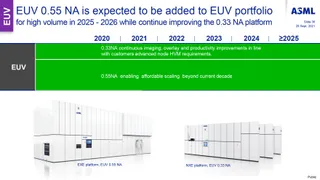
This week, Intel began to receive its first ASML's extreme ultraviolet (EUV) lithography tool with a 0.55 numerical aperture (High-NA), which it will use to learn how to use the technology before deploying such machines for a post-18A production node in the next couple of years or so. By contrast, TSMC is in no rush to adopt High-NA EUV any time soon, and it might be years before the company jumps on this bandwagon in 2030 or beyond, according to analysts from China Renaissance .
"In contrast to Intel's use of High-NA EUV soon after its shift to GAA (planned for [20A] insertion), we expect TSMC'sHigh-NA EUV insertion in the post N1.4 era (the inflection likely at N1, scheduled for post-2030 launch), wrote Szeho Ng, an analyst with China Renaissance.
Intel's aggressive process technology roadmap includes the insertion of RibbonFET gate-all-around (GAA) transistors and PowerVia backside power delivery network (BSPDN) starting from 20A (20 angstroms, 2nm-class), then refining them with 18A , and then start using High-NA EUV tools for a post-18A node to offer the power, performance, and area characteristics and the lowest cycle time.
Modern EUV litho tools equipped with 0.33 numerical aperture lenses (Low-NA) provide an achievable critical dimension in the range of 13 to 16 nm for mass production, which is sufficient to produce a minimum metal pitch of 26 nm, and an estimated 25 to 30 nm tip-to-tip interconnect space pitch using single exposure patterning. This is sufficient for a 3nm-class process technology (with metal pitches between 21 and 24nm), but at 2nm and beyond, metal pitches will shrink to about 18–21nm (according to imec), which will call for the usage of EUV double patterning, pattern shaping equipment , or High-NA single patterning.

Intel plans to insert pattern shaping starting from 20A (which is about to enter HVM) and then High-NA EUV starting from a post-18A node, enabling the company to reduce the complexity of its process flow and avoid the usage of EUV double-patterning. However, High-NA EUV litho tools are significantly more expensive than Low-NA EUV scanners, but the High-NA EUV has many peculiarities, including a 2x reduced exposure field.
As a result, analysts from SemiAnalysis and China Renaissance believe that usage of High-NA EUV machines may be costlier than usage of Low-NA EUV double patterning, at least initially, which is why TSMC might not be inclined to use it for a while to ensure low costs albeit at the cost of production complexities and perhaps lower transistor density.
“Low-NA EUV multiple patterning, despite lower throughput on more exposure passes, may still cost less than high-NA EUV in the initial GAA foray; the higher source power of high-NA EUV to drive finer CD (critical dimension) speeds up wear on projection optics and photomasks, outweighing higher throughput benefits,” explained Szeho Ng. “This ties with TSMC’s practice to target the volume market with the most cost-competitive technologies.”
TSMC began to use extreme ultraviolet (EUV) lithography tools for high-volume production of chips in 2019, months after Samsung Foundry but years before Intel. Intel wants to be ahead of Samsung Foundry and TSMC with High-NA EUV, which could ensure some tactic and strategic benefits. The only question is, will TSMC be able to maintain its process technology leadership if it adopts High-NA litho only in 2030 or later (i.e., four to five years after Intel)?