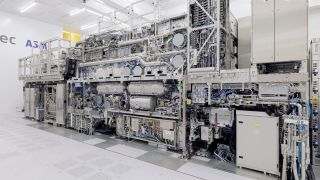
Shrinking transistor dimensions is critical for continued scaling of chip performance, so the semiconductor industry is working on various ways to make transistors smaller. In the coming years, chipmakers are set to adopt ASML's latest high-NA extreme ultraviolet (EUV) lithography tools, which will be particularly useful for post-3nm-class fabrication nodes. But what's next? ASML says that Hyper-NA is currently being explored for as-yet-undefined new tools that would arrive in the 2030s to power future generations of chips.
"Hyper-NA with an NA higher than 0.7 is certainly an opportunity that will become more visible from around 2030," wrote Martin van den Brink, chief technology officer of ASML, in ASML's 2023 Annual Report (via Bits & Chips ). "It is likely to be most relevant for Logic — and it will need to be more affordable than [High-NA EUV] double patterning — but it may also be an opportunity for DRAM. For us, the key thing is that Hyper-NA is driving our overall EUV capability platform to improve both cost and lead time."
ASML's current crop of EUV tools consists of Low-NA models, which feature 0.33 NA optics and can achieve a critical dimension (CD) of 13.5 nm. That's sufficient to produce a minimum metal pitch of 26 nm and an approximate interconnect space pitch of 25–30nm tip-to-tip with a single exposure patterning. These dimensions are good enough for 4nm/5nm-class production nodes. Still, the industry will need 21-24nm pitches for 3nm, which is why TSMC's N3B process technology is designed to use Low-NA EUV double patterning to print the smallest possible pitches. This approach is considered very expensive.
Next-gen High-NA EUV systems with 0.55 NA optics will achieve a CD of 8nm, which will be enough to print a minimum metal pitch of around 16nm, which will be useful for nodes beyond 3nm and is expected to be good enough even for 1nm, at least according to figures envisioned by Imec .

But metal pitches will get even smaller beyond 1nm, so the industry will need more sophisticated tools than ASML's High-NA devices. This leads us to Hyper-NA tools with even higher numerical aperture projection optics. ASML's CTO, Martin van den Brink, confirmed in an interview with Bits & Chips that the viability of Hyper-NA technology is being investigated. Still, no final decision has been made yet.
Increasing the numerical aperture of projection optics is a costly process involving significant changes to the design of the lithography tools. In particular, this includes the machine's physical dimensions, the need to develop many new components, and the impact of increased costs. A Low-NA EUV Twinscan NXE machine costs $183 million or higher depending on configuration, and a High-NA EUV Twinscan EXE tool will be priced at $380 million or higher depending on configuration, ASML recently disclosed . Hyper-NA would cost more than that, so ASML has to answer two questions: whether it can be done technologically and whether it will be economically viable for the leading logic chipmakers.
Only three leading-edge chipmakers are left: Intel, Samsung Foundry, and TSMC. Japan-based Rapidus has yet to develop into a feasible competitor. So, while Hyper-NA EUV lithography is needed, it has to be reasonably affordable.
"The introduction of Hyper-NA will be determined by the extent to which we can reduce costs," Martin van den Brink told Tweakers.net last year. "I have traveled around the world several times and have spoken with customers about the necessity and desirability of Hyper-NA. In recent months, I have gained the confidence and insight that customers want to drive the resolution down so much further, that the possibility for the use of Hyper-NA for mass production of logic and memory chips is there. That would be around the next decade change. But it depends on the costs."