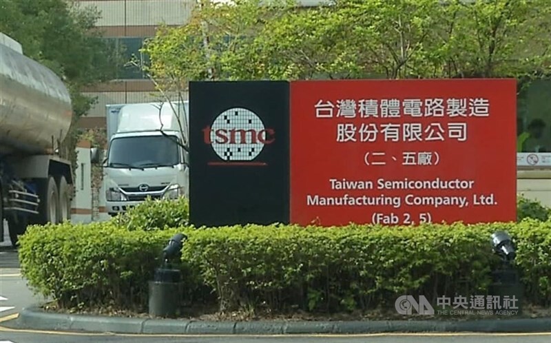
TSMC is expected to risk-produce chips on its 2 nm node in its new fab at the Baoshan campus in the Hsinchu Science Park, located in northern Taiwan. Should all go well with risk production, one can expect mass production of chips by Q2-2025. Until then, refinements to the company's final FinFET node, the N3 family, will remain the cutting-edge of silicon fabrication. Samsung has a similar 2025 target set for mass production on its 2 nm node, dubbed SF2. Across the Pacific, Intel Foundry Services has its Intel 20A node, which implements GAAFET (aka RibbonFET) technology aiming for similar timelines, including an ambitious 2024 mass production target.