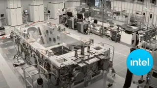
Late last year ASML started to ship its first High-NA extreme ultraviolet (EUV) lithography system to Intel, and this past weekend the processor giant published a video covering installation of the tool into its fab near Hillsboro, Oregon. The machine will be used primarily for research and development purposes.
ASML's Twinscan EXE:5000 High-NA EUV machine is indeed huge. It took a cargo plane to transport it from The Netherlands to Portland, Oregon, and then a truck to deliver one of the key components of the tool. The unit has been installed at the fab, but it will take 250 ASML and Intel engineers about six months' time to install all the components of the device.
But even when the Twinscan EXE:5000 High-NA EUV machine, with a 0.55 numerical aperture projection optics, is fully assembled, ASML and Intel engineers will need to calibrate it, which will take weeks if not months. At first, the two companies will have to 'light up' the device, which is when photons hit resist on wafers, something that ASML engineers recently achieved with their High-NA EUV tool in Veldhofen, the Netherlands.
ASML's High-NA EUV Twinscan EXE tools is set to achieve an 8nm resolution, significantly enhancing the performance of currently used Low-NA EUV scanners, which are limited to 13nm resolution with a single exposure. This advancement enables building transistors that are about 1.7 times smaller than today, resulting in almost triple the transistor density. Achieving 8nm critical dimensions is crucial for producing chips using sub-3nm process technologies, a target the industry hopes to reach between 2025 and 2026.
Intel will use its Twinscan EXE:5000 lithography tool mainly to learn how to use High-NA EUV technology. The company plans to test the usage of High-NA lithography with its Intel 18A process technology (albeit not for high-volume production) and eventually adopt it for high-volume manufacturing with its Intel 14A fabrication process.
ASML previously announced that its next-generation High-NA EUV chipmaking tool would be more than double the price of its current Low-NA EUV lithography tools, approximately $380 million (€350 million), though exact price will depend on actual configuration of the device, and Intel CEO Pat Gelsinger has said that the machine cost '400-ish million.'
In comparison, existing Low-NA Twinscan NXE EUV systems are priced at around $183 million (€170 million), with variations based on specific models and configurations. Intel may be one of the first to receive this cutting-edge fabrication tool, but ASML has disclosed “10 to 20” orders for its High-NA EUV machines so far, from companies like Intel, Samsung, SK Hynix, and TSMC.