Please note that this post is tagged as a rumor .
NVIDIA RTX 5090 with significantly higher base clock
Chiphell leaker Panzerlied claims that the RTX 5090 may see much improved base frequency.

Discussion on Chiphell forums has led to new details about the RTX 5090 graphics card. Panzerlied, who previously revealed that the RTX 5090 will use a 448-bit memory bus, now claims the base GPU frequency will be over 600 MHz higher than the RTX 4090.
According to the leaker, the RTX 5090 will feature an “almost 2.9 GHz” base clock, significantly higher than the RTX 4090’s 2.23 GHz. This base clock even surpasses the current flagship’s boost clock of 2.52 GHz. However, this does not confirm that the boost clock will also be much higher, as it is uncertain if NVIDIA has changed how it handles clock speeds in the Blackwell-based gaming GPUs. However, it seems likely that we will see a 3 GHz boost clock on the next-gen flagship model.

RTX 5090 with 2.9 GHz base clock, Source: Chiphell
According to rumors, the RTX 5090 will feature the GB202 Blackwell GPU with an unconfirmed configuration. The full chip is expected to have 192 Streaming Multiprocessors, resulting in 24,000 cores if NVIDIA maintains the same FP32 core count as their previous gaming Blackwell GPUs.
Additionally, the card is expected to include 28GB of GDDR7 memory on a 448-bit memory bus. With the memory clocked at 28 Gbps, this configuration would offer over 1.5 TB/s of bandwidth, representing a 50% increase over the RTX 4090.
GeForce RTX 5090 spec rumors
- GPU : GB202
- Memory : 28GB GDDR7 448-bit 28 Gbps
- Base Clock : ~2.9 GHz 🆕
- Announcement : Late 2024
So far, everything suggests that the RTX 5090 will be a significant upgrade over the RTX 4090, featuring more cores and memory, higher bandwidth, and significantly higher clock speeds. If NVIDIA manages to maintain the same launch price, it would already be major news.
| NVIDIA RTX 5090 vs. 4090 | ||
|---|---|---|
| VideoCardz.com | RTX 5090 FE | RTX 4090 FE |
| Picture | [To be Leaked] | 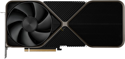 |
| GPU | GB202 | AD102 |
| Architecture | Blackwell | Ada Lovelace |
| Total SMs | Less than 192 | 128 |
| CUDA Cores (Assumed) | Less than 24576 | 16384 |
| Base Clock | ~2.9 GHz | ~2.23 GHz |
| Boost Clock | TBC | ~2.52 GHz |
| Memory | 28 GB GDDR7 | 24 GB GDDR6X |
| Memory Bus | 448-bit | 384-bit |
| Memory Speed | 28 Gbps | 21 Gbps |
| Memory Bandwidth | 1568 GB/s | 1008 GB/s |
| Power Connectors | 1x 12VHWPR (16-pin) (?) | 1x 12VHWPR (16-pin) |
| Default TGP | TBC | 450W |
| Founders Edition Design | 2-slot, dual-fan | 3-slot, dual-fan |
| MSRP | TBC | 1599 USD |
| Announcement Date | Late 2024 | October 12th, 2022 |
Source: Chiphell