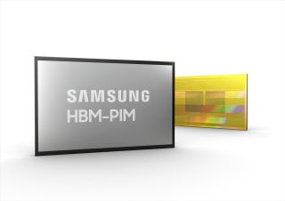
Today, Samsung announced that its new HBM2-based memory has an integrated AI processor that can push out (up to) 1.2 TFLOPS of embedded computing power, allowing the memory itself to perform operations that are usually reserved for CPUs, GPUs, ASICs, or FPGAs.
The new HBM-PIM (processing-in-memory) chips inject an AI engine inside each memory bank, thus offloading processing operations to the HBM itself. The new class of memory is designed to alleviate the burden of moving data between memory and processors, which is often more expensive in terms of power consumption and time than the actual compute operations.
Samsung says that, when applied to its existing HBM2 Aquabolt memory, the tech can deliver twice the system performance while reducing energy consumption by more than 70%. The company also claims that the new memory doesn't require any software or hardware changes (including the memory controllers), thus enabling a faster time to market for early adopters.
Samsung says the memory is already under trials in AI accelerators with leading AI solutions providers. The company expects all validations to be completed in the first half of this year, marking a speedy path to market.
Samsung presented the finer details of its new memory architecture during the International Solid-State Circuits Virtual Conference (ISSCC) this week.








As you can see in the slides above, the new memory has an embedded Programmable Computing Unit (PCU), which runs at 300 MHz, embedded into each memory bank. This unit is controlled via conventional memory commands from the host to enable in-DRAM computations, and it can execute various FP16 computations. The memory can also operate in either standard mode, meaning it operates as normal HBM2, or in FIM mode for in-memory data processing.
Notably, the paper and slides above refer to the tech as Function-In Memory DRAM (FIMDRAM), but that was an internal codename for the technology that now carries the HBM-PIM brand name.
The paper describes the underlying tech as "Function-In Memory DRAM (FIMDRAM) that integrates a 16-wide single-instruction multiple-data engine within the memory banks and that exploits bank-level parallelism to provide 4× higher processing bandwidth than an off-chip memory solution. Second, we show techniques that do not require any modification to conventional memory controllers and their command protocols, which make FIMDRAM more practical for quick industry adoption."
Unfortunately, we won't see these capabilities in the latest GPUs, at least for now. Samsung notes that the new memory is destined to satisfy large-scale processing requirements in data centers, HPC systems, and AI-enabled mobile applications. As with most in-memory processing techniques, we expect this tech will press the boundaries of the memory chips' cooling and power limitations, especially given that HBM chips are typically deployed in stacks that aren't exactly conducive to easy cooling. Samsung's presentation did not cover how HBM-PIM addresses those challenges.
Kwangil Park, senior vice president of Memory Product Planning at Samsung Electronics stated, "Our groundbreaking HBM-PIM is the industry's first programmable PIM solution tailored for diverse AI-driven workloads such as HPC, training and inference. We plan to build upon this breakthrough by further collaborating with AI solution providers for even more advanced PIM-powered applications."