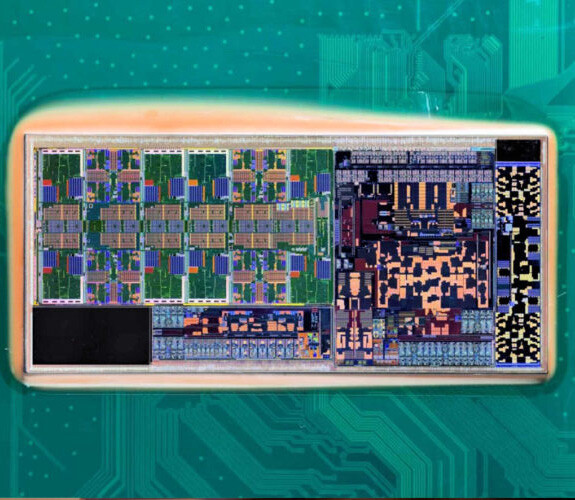
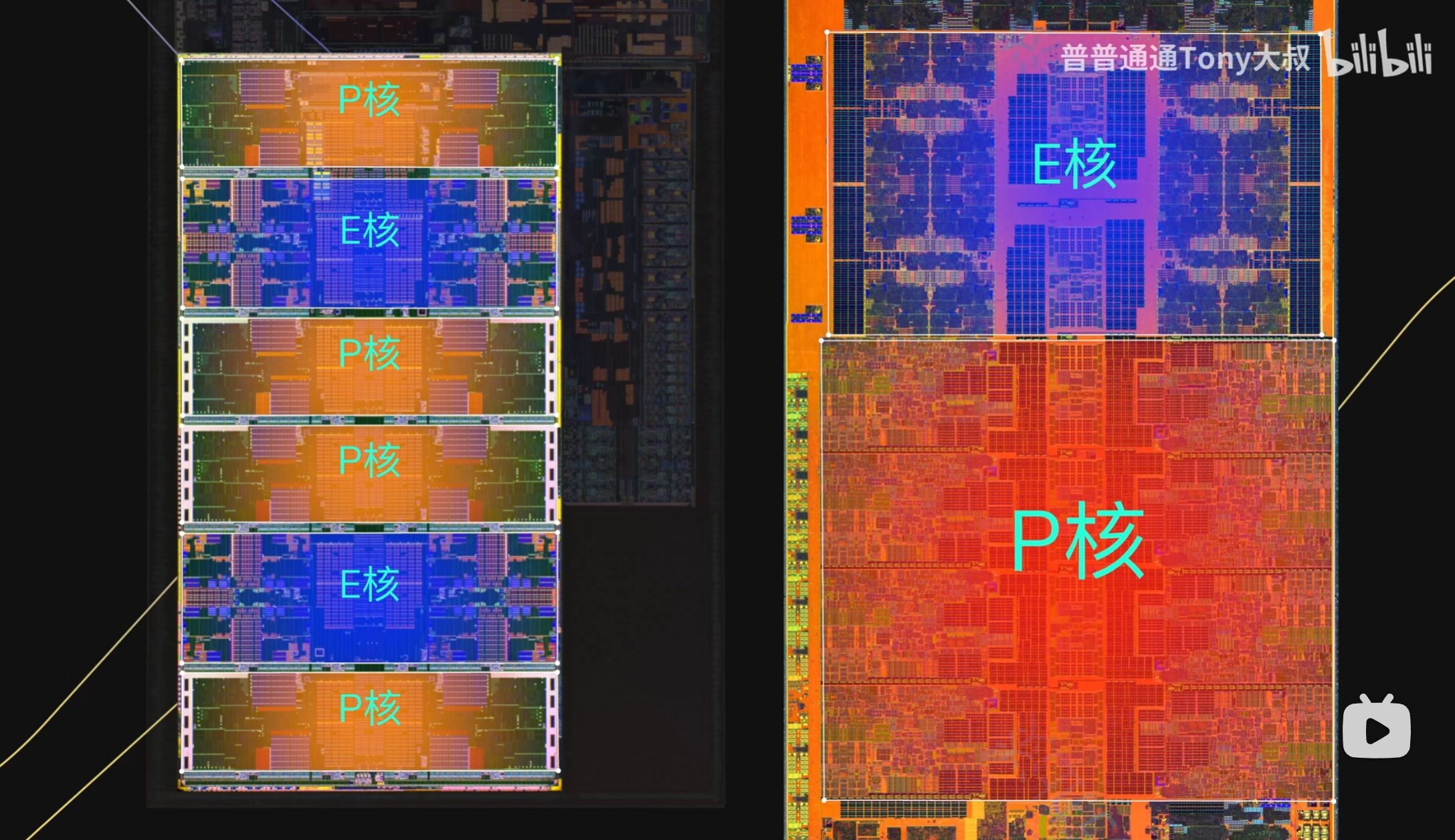
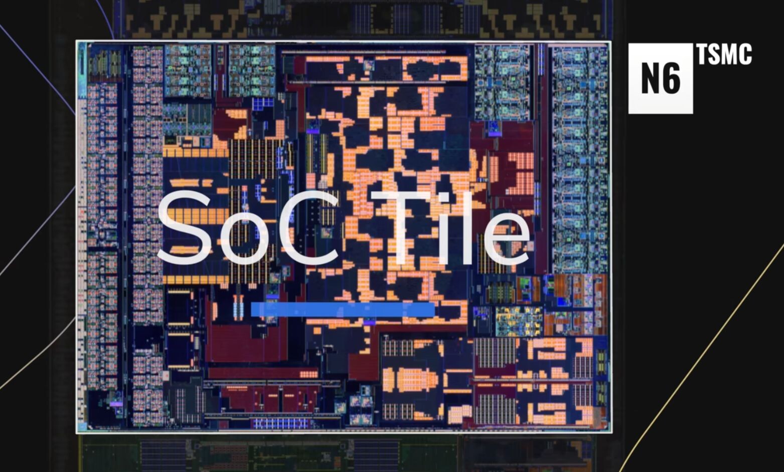
The whole-chip die-shot gives us a bird's eye view of the four key logic tiles—Compute, Graphics, SoC, and I/O, sitting on top of the Foveros base tile. Our article from earlier this week goes into the die areas of the individual tiles, and the base tile. The Compute tile is built on the most advanced foundry node among the four tiles, the 3 nm TSMC N3B. Unlike the older generation "Raptor Lake-S" and "Alder Lake-S," the P-cores and E-core clusters aren't clumped into the two ends of the CPU complex. In "Arrow Lake-S," they follow a staggered layout, with a row of P-cores, followed by a row of E-core clusters, followed by two rows of P-cores, and then another row of E-core clusters, before the final row of P-cores, to achieve the total core-count of 8P+16E. This arrangement reduces concentration of heat when the P-cores are loaded (eg: when gaming), and ensures each E-core cluster is just one ringbus stop away from a P-core, which should improve thread-migration latencies. The central region of the tile has this ringbus, and 36 MB of L3 cache shared among the P-cores and E-core clusters.