The PCB of the Intel DG2 512EU graphics card has been pictured
Moore’s Law is Dead has revealed a back of the PCB for the upcoming Intel DG2 flagship graphics card.
Intel is now heavily engaged in the development of its DG2 family based on Xe-HPG (Gaming) architecture. Moore’s Law is Dead has been frequently publishing information on the series thanks to the confidential sources that provide early information as well as photos of the engineering samples. Last month the leaker revealed the first photos of the Xe-HPG DG2-512EU graphics card , which is the flagship configuration for the upcoming mobile and desktop series. Obviously, the card that was photographed is a discrete desktop form. However, it remains to be seen how much different the engineering sample will be from the final retail version that is now expected to launch in the first quarter of 2022, Moore’s Law is Dead claims.
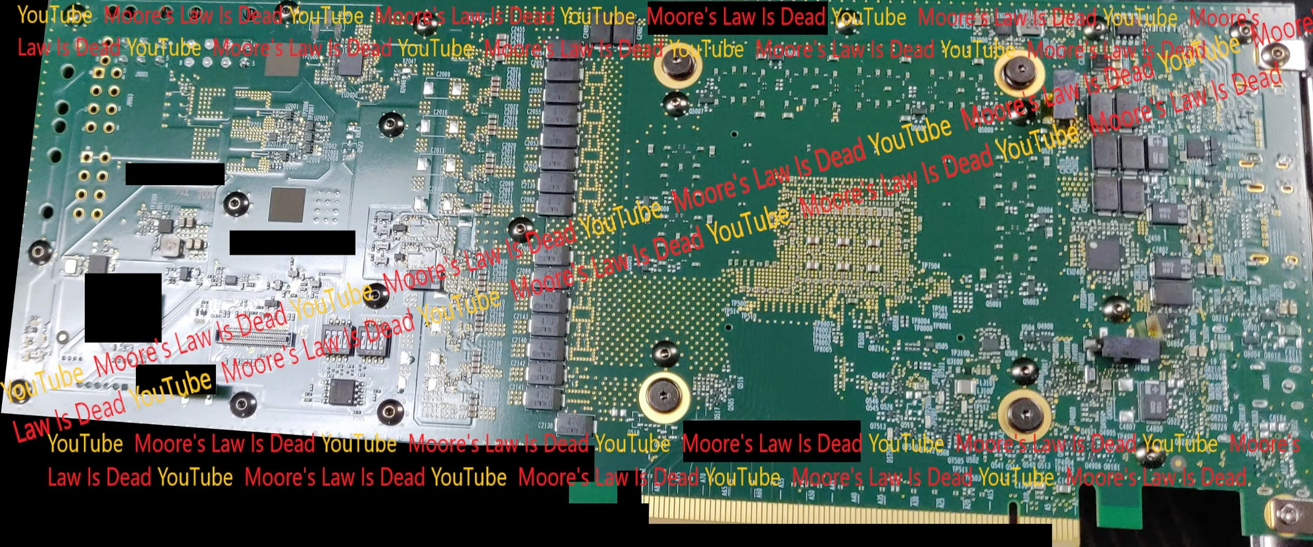
Intel DG2-512EU Engineering Sample, Source: Moore’s Law is Dead
Today the YouTuber revealed the first photo of the graphics card’s PCB. It is not a frontal picture, but of its back, where we can only see the basic component layout. The PCB is much longer than the current NVIDIA RTX 30 series, but this shouldn’t come as surprise considering this is an engineering sample. The PCB supports dual 8-pin power connectors, which are soldered, but there is room for additional pair. This might be a leftover from earlier samples and something that Intel might remove later (this can also help to reduce the size of the PCB).
We have already seen the DG2-128 and DG2-384 diagrams . Those numbers denote the number of Execution Units on each GPU, but in total, there are three GPU variants expected in the DG2 family. The 384EU and 512EU variants will feature the same package, which means that they will occupy the same space on PCB. We made a quick comparison to see if that’s true. The DG2-512EU and 384EU GPUs indeed appear to be identical in size. There is, however, a small difference in memory layout, as the 512EU variant features 8 memory modules (256-bit bus), whereas the 384EU model has 6 (192-bit bus).
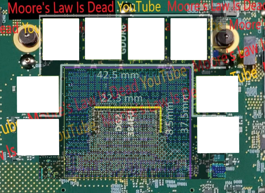
Intel DG2-512EU PCB vs DG2-384EU diagram
This is likely the same card that was already pictured and posted by the leaker last month. We can see that both cards feature green PCB, which is a common theme for engineering samples.

Intel DG2-512EU Engineering Sample, Source: Moore’s Law is Dead
Furthermore, Moore’s Law is Dead claims that at this moment Intel Xe-HPG series is to launch in the first quarter this year. There is a chance that we might see a reveal already in late 2021 though, which is more or less what Intel promised. However, it might be underwhelming that Intel will not compete in high-end desktop and mobile GPU spectrum with AMD and NVIDIA when that competition is needed the most (eg. when no cards are in stock).
YouTuber reaffirms his previous claims that DG2 successor is codenamed “Elasti”. This is probably an internal codename for the DG3 family, which has already appeared in previous leaks. Lastly, it is mentioned that Intel is developing new software for ‘Smooth Frame Delivery’. Judging by its name this could theoretically be Intel’s response to NVIDIA Reflex and Radeon Boost to reduce in-game lag.
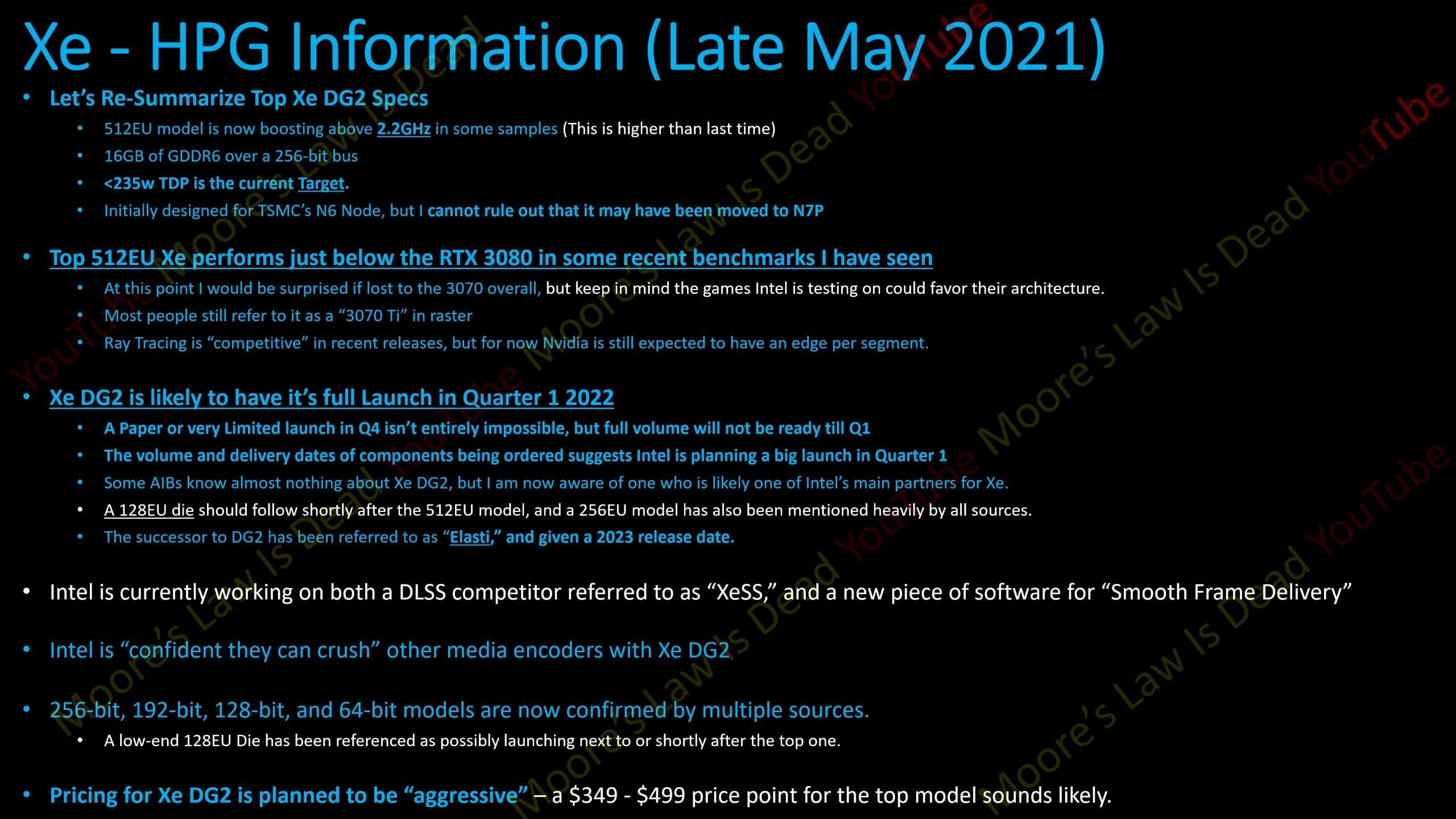
Intel DG2 details, Source: Moore’s Law is Dead
| INTEL DG2 Mobile Gaming Graphics Cards | |||||
|---|---|---|---|---|---|
| SKU1 | SKU2 | SKU3 | SKU4 | SKU5 | |
| Mobile Package | BGA2660 | BGA2660 | BGA2660 | BGA1379 | BGA1379 |
| GPU | DG2-512EU | DG2-384EU | DG2-384EU | DG2-128EU | DG2-128EU |
| Execution Units | 512 | 384 | 256 | 128 | 96 |
| Shading Units | 4096 | 3072 | 2048 | 1024 | 768 |
| Memory | 16GB GDDR6 | 12GB GDDR6 | 8GB GDDR6 | 4GB GDDR6 | 4GB GDDR6 |
| Bus | 256-bit | 192-bit | 128-bit | 64-bit | 64-bit |
| Mobile Base Clock | 1.1 GHz | 0.6 GHz | 0.45 GHz | TBC | TBC |
| Mobile Boost Clock | 1.8 GHz | 1.8 GHz | 1.4 GHz | TBC | TBC |
| Mobile (TGP) | 120W | 80W | 60W | 35W | 25W |
Source: