AMD Aldebaran CDNA2 GPU features two dies
In the most recent Linux kernel update, AMD engineers have confirmed that the upcoming CDNA2 GPU codenamed Aldebaran will feature two dies.

While consumer graphics processing units are not expected to feature MCM (Multi-Chip-Module) design till at least RDNA3 (what rumors seem to suggest), the compute accelerators such as Intel Xe-HP(C), NVIDIA Hopper and AMD CDNA2 architecture will all participate in the MCM revolution.
We have seen rumors that Aldebaran features two compute dies on the package, which were referenced in the Linux updates as die0 and die1, leaving a possibility that there might be more. Today AMD engineering confirmed that only the primary die will handle the power data, which should not be set through ‘secondary die’. This ultimately confirms there are two dies.
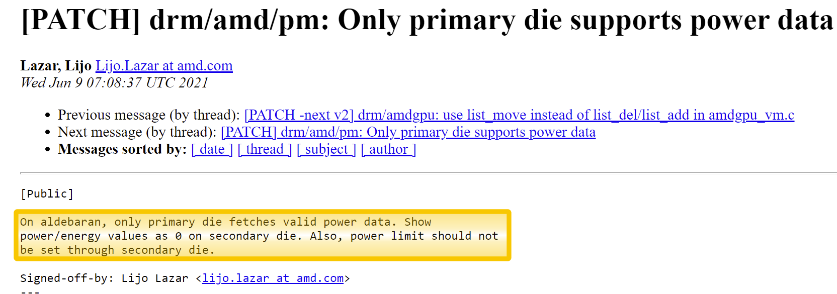
This means that the primary die will regulate the power consumption and power limits for the whole compute part of the package. It is not clear if the power of the HBM2 memory will also be regulated by this die, or by a new I/O module.
The specifications of the Aldebaran MCM package are currently unknown, but it will definitely be a major change from the monolithic Arcturus design. A dual-die configuration will require an interface/interconnect die, which is likely to increase the size of the whole package. AMD is probably going to take a small step before going all-in with more compute dies. Small chips and interposers will require less engineering and should simplify the production.
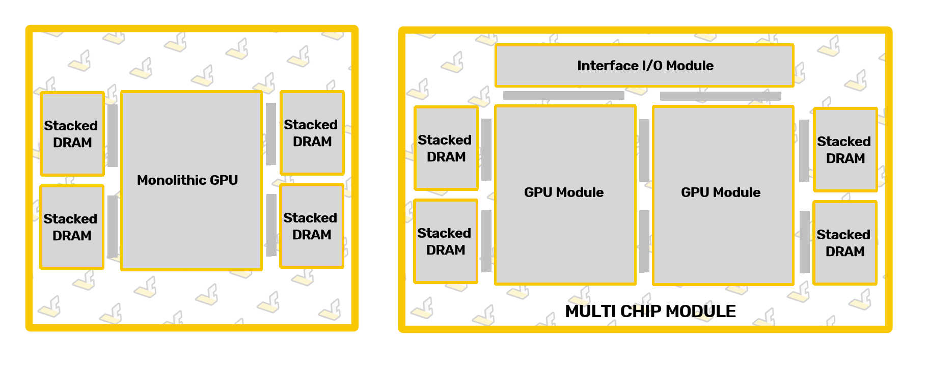
Monolithic vs MCM design, Source: VideoCardz
AMD has never publicly confirmed that CDNA2 will be MCM design, however, the official roadmap did suggest it will have ‘Advanced Node’, which is often how manufacturers refer to product featuring different nodes for each die (in other words not everything will be made in 5nm process technology).
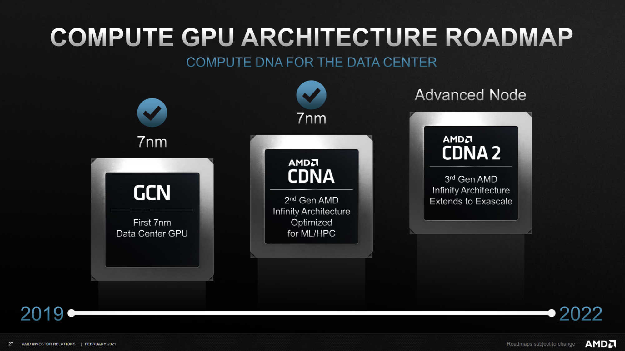
AMD CDNA Roadmap, Source: AMD
AMD Instinct MI200 is likely to launch next year alongside other 5nm products, such as Raphael and RDNA3 consumer graphics. The latter is also rumored to feature an MCM design for at least two GPUs.
| AMD Instinct Accelerators | |||
|---|---|---|---|
| Accelerator Name | AMD Radeon Instinct MI60 | AMD Instinct MI100 | AMD Instinct MI200 |
| Architecture | 7nm GCN5 | 7nm CDNA1 (GFX908) | CDNA2 (GFX90A) |
| GPU | Vega 20 | Arcturus | Aldebaran (MCM) |
| GPU Cores | 4096 | 7680 | TBC |
| GPU Clock Speed | 1800 MHz | ~1500 MHz | TBC |
| FP16 Compute | 29.5 TFLOPs | 185 TFLOPs | TBC |
| FP32 Compute | 14.7 TFLOPs | 23.1 TFLOPs | TBC |
| FP64 Compute | 7.4 TFLOPs | 11.5 TFLOPs | TBC |
| VRAM | 32 GB HBM2 | 32 GB HBM2 | HBM2E |
| Memory Clock | 1000 MHz | 1200 MHz | TBC |
| Memory Bus | 4096-bit bus | 4096-bit bus | TBC |
| Memory Bandwidth | 1 TB/s | 1.23 TB/s | TBC |
| Form Factor | Dual Slot, Full Length | Dual Slot, Full Length | OAM |
| Cooling | Passive Cooling | Passive Cooling | TBC |
| TDP | 300W | 300W | TBC |
Source: Freedesktop via Coelacanth’s Dream