Qualcomm Swaps Out Arm for RISC-V for Next-Gen Google Wear OS Devices

As part of a broad collaborative agreement with Google, Qualcomm this week said that that it will be adopting the RISC-V instruction set architecture (ISA) for a future Snapdragon Wear platform. Working together, the two companies will be bootstrapping a RISC-V ecosystem for Wear OS devices, with Qualcomm providing the hardware while Google expands its wearables OS and associated ecosystem of tools to support the new processor architecture.
Qualcomm's Wear processors have been the de facto chip of choice for Wear OS devices since the launch of
Canon Prepares Nanoimprint Lithography Tool To Challenge EUV Scanners

Canon has recently revealed its FPA-1200NZ2C, a nanoimprint semiconductor manufacturing tool that can be used to make advanced chips. The device uses nanoimprint lithography (NIL) technology as an alternative to photolithography, and can theoretically challenge extreme ultraviolet (EUV) and deep ultraviolet (DUV) lithography tools when it comes to resolution.
Unlike traditional DUV and EUV photolithography equipment that transfers a circuit pattern onto a resist-coated wafer through projection, nanoimprint tool employs a different technique. It uses a mask,
Intel Core i9-14900K, Core i7-14700K and Core i5-14600K Review: Raptor Lake Refreshed
In what is to be the last of Intel's processor families to use the well-established Core i9, i7, i5, and i3 naming scheme, Intel has released its 14th Generation Core series of desktop processors, aptly codenamed Raptor Lake Refresh (RPL-R). Building upon the already laid foundations of the 13th Gen Core series family, Intel has announced a variety of overclockable K and KF (no iGPU) SKUs, including the flagship Core i9-1
Intel Announces 14th Gen Core Series For Desktop: Core i9-14900K, Core i7-14700K and Core i5-14600K
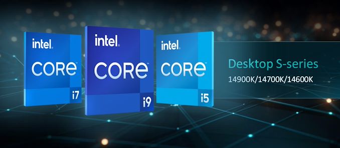
Ahead of tomorrow's full-scale launch, Intel this afternoon is pre-announcing their 14th Generation Core desktop processors. Aptly codenamed Raptor Lake Refresh , these new chips are based on Intel's existing Raptor Lake silicon – which was used in their 13th generation chips – with Intel tapping further refinements in manufacturing and binning in order to squeeze out a little more performance from the silicon. For their second iteration of Raptor Lake, Intel is also preserving their pricing for the Core i9, i
TSMC: We Want OSATs to Expand Their Advanced Packaging Capability
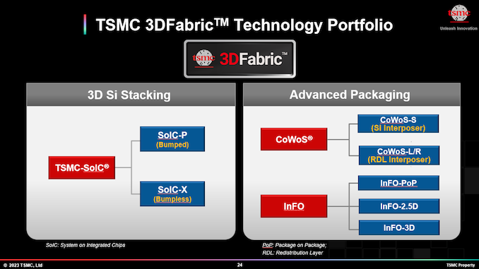
Almost since the inception of the foundry business model in the late 1980s, TSMC would produce silicon. In contrast, an outsourced semiconductor assembly and test (OSAT) service provider would then package it into a ceramic or organic encasing. Things have changed in recent years with the emergence of advanced packaging methods that require sophisticated tools and cleanrooms that are akin to those used for silicon production because TSMC was at the forefront of innovative packaging methods, which the company aggregates under the 3DFabric brand and because it built
GEEKOM Mini IT13 Review: Core i9-13900H in a 4x4 Package
The performance of ultra-compact form-factor (UCFF) desktops has improved significantly over the years, thanks to advancements in semiconductor fabrication and processor architecture. Thermal solutions suitable for these 4in. x 4in. machines have also been evolving simultaneously. As a result, vendors have been able to configure higher sustained power limits for the processors in these systems. With Intel and AMD allowing configurable TDPs for their notebook segment offerings, UCFF systems with regular 45W TDP processors (albeit, in cTDP-down mode
TSMC: Ecosystem for 2nm Chip Development Is Nearing Completion
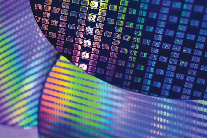
Speaking to partners last week as part of their annual Open Innovation Platform forum in Europe, a big portion of TSMC's roadshow was dedicated to the next generation of the company's foundry technology. TSMC's 2 nm-class N2 , N2P, and N2X process technologies are set to introduce multiple innovations, including nanosheet gate-all-around (GAA) transistors, backside power delivery, and super-high-performance metal-insulator-metal (SHPMIM) capacitor over the next
Samsung Lines Up First Server Customer For 3nm Fabs

Although Samsung Foundry was the first contract fab to formally start mass production of chips on a 3 nm-class process, so far, the company's latest process has largely been relegated to producing tiny cryptocurrency mining chips. But it looks like things will start picking up for Samsung's foundry business soon, as this week it was announced that the company has landed a more substantial order which will see the Samsung make a server-grade system-in-package (SiP) with HBM memory for an unknown client
HBM4 in Development, Organizers Eyeing Even Wider 2048-Bit Interface
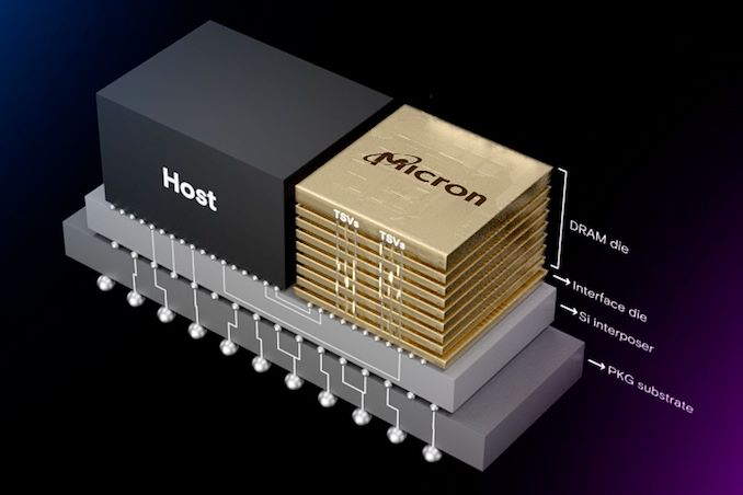
High-bandwidth memory has been around for about a decade, and throughout its its continued development it has steadily increased in speed, starting at a data transfer rate from 1 GT/s (the original HBM) and reaching upwards of 9 GT/s with the forthcoming HBM3E. This has made for an impressive jump in bandwidth in less than 10 years, making HBM an important cornerstone for whole new classes of HPC accelerators that have since hit the market. But it's also a pace that'
TSMC: Importance of Open Innovation Platform Is Growing, Collaboration Needed for Next-Gen Chips
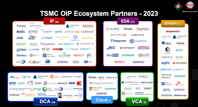
This year TSMC is commemorating 15 years of its Open Innovation Platform, a multi-faceted program that brings together the foundry's suppliers, partners, and customers to help TSMC's customers better build innovative chips in an efficient and timely manner. The OIP program has grown over the years and now involves tens of companies and over 70,000 IP solutions for a variety of applications. It continues to grow, and its importance will get higher than ever when next generation technologies, such as 2