Samsung Starts 3nm Production: The Gate-All-Around (GAAFET) Era Begins
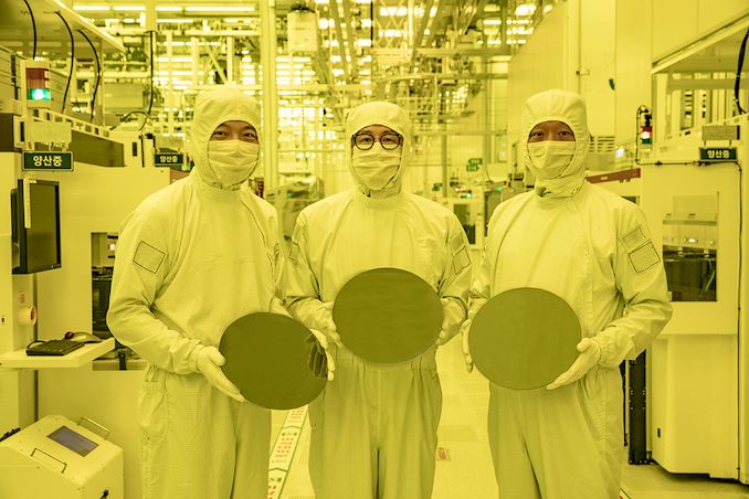
Capping off a multi-year development process, Samsung’s foundry group sends word this morning that the company has officially kicked off production on its initial 3nm chip production line. Samsung’s 3nm process is the industry’s first commercial production process node using gate-all-around transistor (GAAFET) technology, marking a major milestone for the field of silicon lithography, and potentially giving Samsung a major boost in its efforts to compete with TSMC.
The relatively spartan announcement from Samsung , which comes on the
ASRock Releases Raptor Lake BIOS Updates For Its 600 Series Motherboards
While Intel has yet to officially announce its next (13th) generation of Core processors, this isn't stopping motherboard manufacturers from releasing products for them. Always eager to slide ahead of the competition and spur on new sales towards the later half of a platform's lifecycle, mobo makers are already releasing BIOSes that support Intel's future chips – parts which, officially speaking, don't even exist (yet).
Leading this charge is ASRock, who today has released a wave of new BIOSes
TSMC: N2 To Start With Just GAAFETs, Add Backside Power Delivery Later
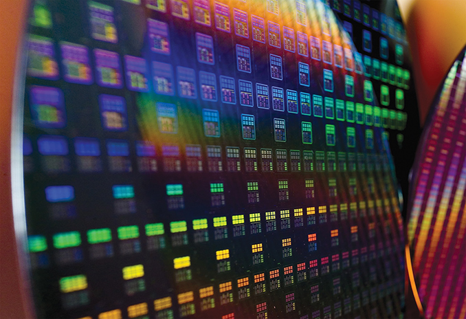
When TSMC initially introduced its N2 (2 nm class) process technology earlier this month, the company outlined how the new node would be built on the back of two new cutting-edge fab techniques: gate-all-around transistors, and backside power rails. But, as we've since learned from last week's EU symposium, TSMC's plans are a bit more nuanced than first announced. Unlike some of their rivals, TSMC will not be implementing both technologies in the initial version of their
TSMC to Customers: It's Time to Stop Using Older Nodes and Move to 28nm
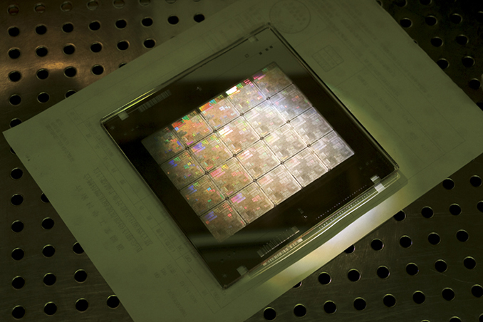
We tend to discuss leading-edge nodes and the most advanced chips made using them, but there are thousands of chip designs developed years ago that are made using what are now mature process technologies that are still widely employed by the industry. On the execution side of matters, those chips still do their jobs as perfectly as the day the first chip was fabbed which is why product manufacturers keep building more and more using them. But on the manufacturing side of matters there's a hard bottleneck to further growth: all
As HPC Chip Sizes Grow, So Does the Need For 1kW+ Chip Cooling
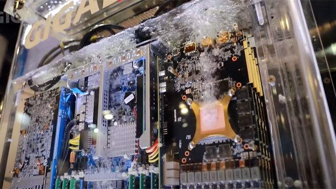
One trend in the high performance computing (HPC) space that is becoming increasingly clear is that power consumption per chip and per rack unit is not going to stop with the limits of air cooling. As supercomputers and other high performance systems have already hit – and in some cases exceeded these limits – power requirements and power densities have continued to scale up. And based on the news from TSMC's recent annual technology symposium, we should expect to see this trend continue as TSMC lays the groundwork for even denser chip configurations
The Gigabyte UD1000GM PG5 1000W PSU Review: Prelude to ATX 3.0
In today's review, we are taking a look at the first-ever PSU released with the new 12VHPWR connector, the GIGABYTE UD1000GM PG5. Although the unit is not ATX v3.0 compliant, GIGABYTE upgraded one of their currently available platforms to provide for a single 600W video card connector in an effort to entice early adopters.
AMD Updates Ryzen Embedded Series, R2000 Series With up to Four Cores and Eight Threads
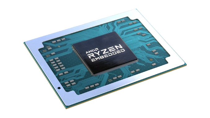
One area of AMD's portfolio that perhaps doesn't garner the same levels of attention as its desktop, mobile, and server products is its embedded business. In early 2020, AMD unveiled its Ryzen Embedded R1000 platform for the commercial and industrial sectors and the ever-growing IoT market, with low-powered processors designed for low-profile systems to satisfy the mid-range of the market.
At Embedded World 2022 in Nuremberg, Germany, AMD has announced
Lenovo ThinkStation P360 Ultra Melds Desktop Alder Lake and NVIDIA Professional Graphics
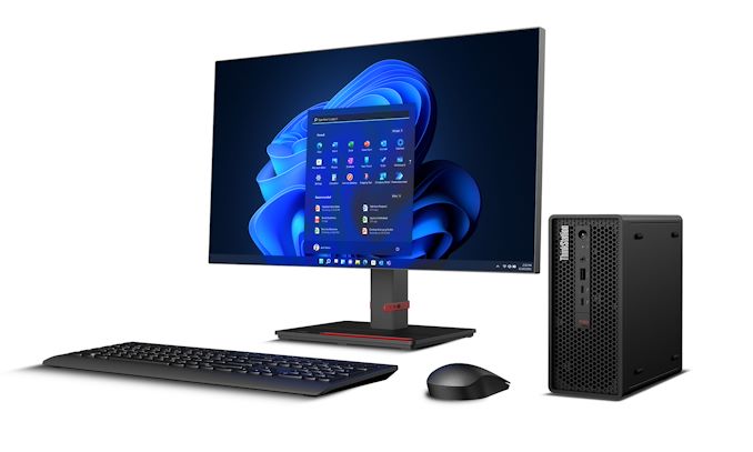
Over the last decade or so, advancements in CPU and GPU architectures have combined extremely well with the relentless march of Moore's Law on the silicon front. Together, these have resulted in hand-held devices that have more computing power than huge and power-hungry machines from the turn of the century. On the desktop front, small form-factor (SFF) machines are now becoming a viable option for demanding professional use-cases. CAD, modeling, and simulation capabilities that required big iron servers or massive
TSMC to Expand Capacity for Mature and Specialty Nodes by 50%
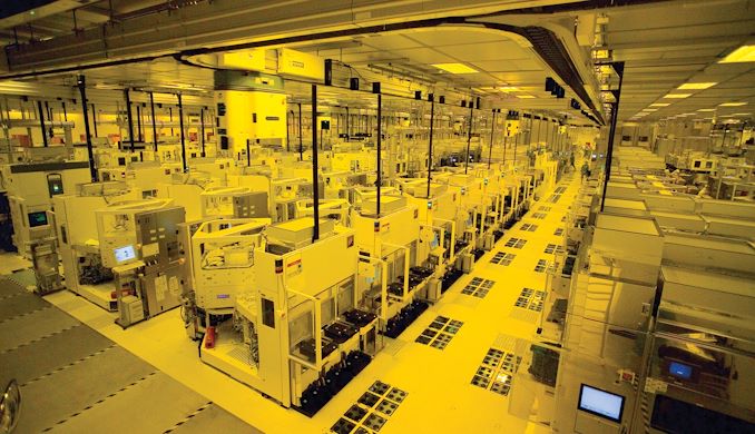
TSMC this afternoon has disclosed that it will expand its production capacity for mature and specialized nodes by about 50% by 2025. The plan includes building numerous new fabs in Taiwan, Japan, and China. The move will further intensify competition between TSMC and such contract makers of chips as GlobalFoundries, UMC, and SMIC.
When we talk about silicon lithography here at AnandTech, we mostly cover leading-edge nodes used produce advanced CPUs, GPUs, and mobile SoCs, as these are devices that drive progress
TSMC Unveils N2 Process Node: Nanosheet-based GAAFETs Bring Significant Benefits In 2025
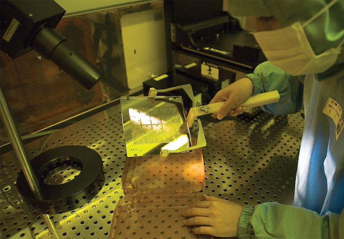
At its 2022 Technology Symposium, TSMC formally unveiled its N2 (2 nm class) fabrication technology, which is slated to go into production some time in 2025 and will be TSMC's first node to use gate-all-around field-effect transistors (GAAFETs). The new node will enable chip designers to significantly reduce the power consumption of their products, but the speed and transistor density improvements seem considerably less tangible.
TSMC's N2 is a brand-new platform