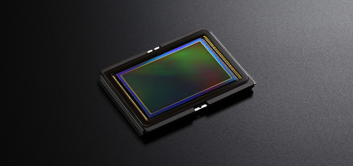
The new company will combine Sony’s expertise in image sensor design with TSMC’s advanced semiconductor manufacturing technology, further strengthening the long-term collaboration between the two firms.
Sony will hold the majority stake in the venture, which will establish development and manufacturing lines at Sony’s new semiconductor facility in Koshi City, located in Japan’s Kumamoto region.
Both companies confirmed they have signed a non-binding memorandum of understanding and are currently discussing the scale of future investments. Final details will depend on a definitive agreement and standard regulatory approvals.
Additional investments are also planned for Sony’s existing Nagasaki plant, with spending expected to increase gradually depending on market demand and potential support from the Japanese government.
Beyond imaging, the partnership will also investigate opportunities in “physical AI” fields such as automotive systems and robotics.
Sony has previously stated that it is open to outside investment in its semiconductor business, emphasizing the massive costs required to stay competitive in chip manufacturing.
Sony and TSMC already cooperate through JASM (Japan Advanced Semiconductor Manufacturing), a separate joint venture founded in 2021 and majority-owned by TSMC. JASM’s first Japanese fab entered mass production at the end of 2024.
**This post contains affiliate links to eBay and I will be compensated if you make a purchase after clicking through my links. As an eBay Associate I earn from qualifying purchases